


L50 Hardware Design
L50_HD_V1.0 -11-
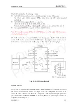
2.2 Functional Diagram
The block diagram of L50 is shown in the Figure 1.
RF Front-
End With
Integrated LNA
Fractional-N
Synthesizer
GPS
Engine
ROM
Saw
Filter
Power
Management
ARM7
Processor
Peripheral
Controller
RTC
VCC
VIO/RTC
UART/I2C
RESET
EINT0
1PPS
ON/OFF
Optional
EEPROM
For CGEE
DR_I2C
Match
Network
RAM
LNA
PATCH
ANTENNA
Figure 1: Functional diagram for L50
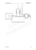
2.3 Evaluation Board
In order to help customers to develop applications with L50, Quectel offers an Evaluation Board (EVB)
with appropriate power supply, RS-232 serial port and EEPROM.
Note: For more details, please refer to the document [1]
.
2.4 Protocol
L50 supports standard NMEA-0183 protocol and the One Socket Protocol (OSP), which is the binary
protocol interface that enables customers’ host device to access all SiRF GPS chip products of the
SiRF Star IV family and beyond. The module is capable of supporting the following NMEA formats:
GGA, GSA, GLL, GSV, RMC, and VTG.
.
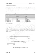
Table 4: The module supports protocols
Protocol
Type
NMEA
Input/output, ASCII, 0183, 3.01
OSP
Input/output, OSP protocol
Note: Please refer to document [2] about NMEA standard protocol and SiRF private protocol.
Quectel
Preliminary
Содержание L50
Страница 1: ...L50 Hardware Design L50 Quectel GPS Engine Hardware Design L50_HD_V1 0 ...
Страница 27: ...L50 Hardware Design L50_HD_V1 0 26 Figure 13 Reference design for CGEE function Quectel Preliminary ...
Страница 30: ...L50 Hardware Design L50_HD_V1 0 29 Figure 15 EVB of L50 Quectel Preliminary ...