background image


                                                                                                  LTE  Standard  Module  Series


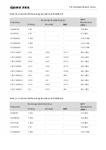
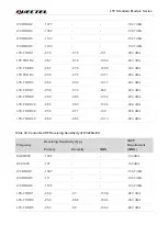
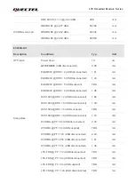
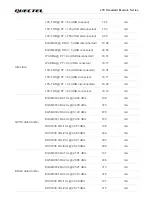
LTE-FDD @ PF = 256 (USB disconnected) 

TBD 

mA 

LTE-TDD @ PF = 32 (USB disconnected) 

TBD 

mA 

LTE-TDD @ PF = 64 (USB disconnected) 

TBD 

mA 

LTE-TDD @ PF = 64 (USB suspend) 

TBD 

mA 

LTE-TDD @ PF = 128 (USB disconnected) 

TBD 

mA 

LTE-TDD @ PF = 256 (USB disconnected) 

TBD 

mA 

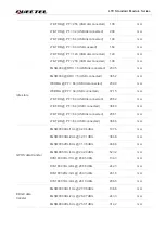
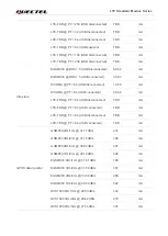
Idle state 

EGSM900 @ DRX = 5 (USB disconnected) 

62.62 

mA 

EGSM900 @ DRX = 5 (USB connected) 

38.93 

mA 

WCDMA @ PF = 64 (USB disconnected) 

14.55 

mA 

WCDMA @ PF = 64 (USB connected) 

39.48 

mA 

LTE-FDD @ PF = 64 (USB disconnected) 

TBD 

mA 

LTE-FDD @ PF = 64 (USB connected) 

TBD 

mA 

LTE-TDD @ PF = 64 (USB disconnected) 

TBD 

mA 

LTE-TDD @ PF = 64 (USB connected) 

TBD 

mA 

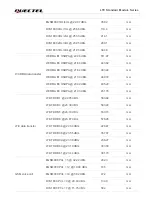
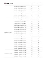
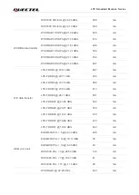
GPRS data transfer 

GSM850 4DL/1UL @ 31.77 dBm 

231 

mA 

GSM850 3DL/2UL @ 31.79 dBm 

389 

mA 

GSM850 2DL/3UL @ 30.80 dBm 

497 

mA 

GSM850 1DL/4UL @ 29.19 dBm 

548 

mA 

EGSM900 4DL/1UL @ 31.61 dBm 

189 

mA 

EGSM900 3DL/2UL @ 31.59 dBm 

357 

mA 

EGSM900 2DL/3UL @ 30.58 dBm 

466 

mA 

EGSM900 1DL/4UL @ 28.99 dBm 

522 

mA 

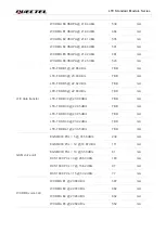
DCS1800 4DL/1UL @ 28.53 dBm 

144 

mA 

DCS1800 3DL/2UL @ 28.42 dBm 

270 

mA 

DCS1800 2DL/3UL @ 27.54 dBm 

331 

mA 

Содержание EC200A Series

Страница 1: ...EC200A Series Hardware Design LTE Standard Module Series Version 1 0 0 Date 2021 11 12 Status Preliminary ...

Страница 2: ...le efforts to provide the best possible experience you hereby acknowledge and agree that this document and related services hereunder are provided to you on an as available basis We may revise or restate this document from time to time at our sole discretion without any prior notice to you Copyright Our and third party products hereunder may contain copyrighted material Such copyrighted material s...

Страница 3: ... designated servers Quectel strictly abiding by the relevant laws and regulations shall retain use disclose or otherwise process relevant data for the purpose of performing the service only or as permitted by applicable laws Before data interaction with third parties please be informed of their privacy and data security policy Disclaimer a We acknowledge no liability for any injury or damage arisi...

Страница 4: ... on sensitive medical equipment so please be aware of the restrictions on the use of wireless devices when in hospitals clinics or other healthcare facilities Cellular terminals or mobiles operating over radio signal and cellular network cannot be guaranteed to connect in certain conditions such as when the mobile bill is unpaid or the U SIM card is invalid When emergent help is needed in such con...

Страница 5: ...tandard Module Series About the Document Revision History Version Date Author Description 2021 11 12 Anthony LIU Kexiang ZHANG Creation of the document 1 0 0 2021 11 12 Anthony LIU Kexiang ZHANG Preliminary ...

Страница 6: ...up Function 25 3 2 2 1 USB Application with USB Suspend Resume and RI Function 27 3 2 2 2 USB Application without USB Suspend Function 27 3 3 Airplane Mode 28 3 4 Power Supply 29 3 4 1 Power Supply Pins 29 3 4 2 Reference Design for Power Supply 29 3 4 3 Requirements for Voltage Stability 30 3 5 Turn On 32 3 5 1 Turn on the Module with PWRKEY 32 3 6 Turn Off 33 3 6 1 Turn off the Module with PWRKE...

Страница 7: ...r Recommendation 64 6 Electrical Characteristics and Reliability 66 6 1 Absolute Maximum Ratings 66 6 2 Power Supply Ratings 67 6 3 Power Consumption 68 6 4 Digital I O Characteristic 78 6 5 ESD 79 6 6 Operating and Storage Temperatures 80 7 Mechanical Information 81 7 1 Mechanical Dimensions 81 7 2 Recommended Footprint 83 7 3 Top and Bottom Views 84 8 Storage Manufacturing and Packaging 85 8 1 S...

Страница 8: ...ADC Interface 48 Table 21 Characteristics of ADC Interface 49 Table 22 Pin Definition of Indication Signal 49 Table 23 Working State of the Network Connection Status Activity Indication 50 Table 24 Behaviors of the MAIN_RI 52 Table 25 Pin Definition of Cellular Network Interface 53 Table 26 Operating Frequency of EC200A CN 53 Table 27 Operating Frequency of EC200A AU 54 Table 28 Operating Frequenc...

Страница 9: ...Series Table 42 Recommended Thermal Profile Parameters 87 Table 43 Carrier Tape Dimension Table Unit mm 89 Table 44 Plastic Reel Dimension Table Unit mm 90 Table 45 Related Documents 91 Table 46 Terms and Abbreviations 91 ...

Страница 10: ...onnector 41 Figure 21 Reference Circuit of U SIM Interface with a 6 pin U SIM Card Connector 42 Figure 22 Timing Sequence for Short frame mode 43 Figure 23 PCM and I2C Interface Circuit Reference Design 44 Figure 24 Reference Circuit with Translator Chip 46 Figure 25 Reference Circuit with Transistor Circuit 46 Figure 26 Reference Circuit of SD Card Interface 47 Figure 27 Reference Circuit of the ...

Страница 11: ...LTE Standard Module Series Figure 43 Plastic Reel Dimension Drawing 89 Figure 44 Packaging Process 90 ...

Страница 12: ...ument is applicable to the following modules EC200A CN EC200A AU EC200A EU 1 1 Special Marks Table 1 Special Marks Mark Definition Unless otherwise specified when an asterisk is used after a function feature interface pin name AT command or argument it indicates that the function feature interface pin AT command or argument is under development and currently not supported and the asterisk after a ...

Страница 13: ...unctionality for your specific applications EC200A series contains 3 variants EC200A CN EC200A AU and EC200A EU You can choose a dedicated type based on the region or operator The following table shows the frequency bands of EC200A series module Table 2 Brief Introduction of the Module Categories Packaging and pins number LCC 80 pin LGA 64 pin Dimensions 29 0 0 15 mm 32 0 0 15 mm 2 4 0 2 mm Weight...

Страница 14: ...ess Network Type Wireless Network Type EC200A CN EC200A AU EC200A EU LTE FDD B1 B3 B5 B8 B1 B2 B3 B4 B5 B7 B8 B28 B66 B1 B3 B5 B7 B8 B20 B28 LTE TDD B34 B38 B39 B40 B41 B40 B38 B40 B41 WCDMA B1 B5 B8 B1 B2 B4 B5 B8 B1 B5 B8 GSM 900 1800 MHz 850 900 1800 1900 MHz 900 1800 MHz ...

Страница 15: ...ts short frame Supports master and slave modes I2C Interface Supports one digital I2C interface Complies with I2C bus protocol specifications 100 400 kHz The multi host mode is not supported USB Interface Compliant with USB 2 0 specification slave only the data transfer rate can reach up to 480 Mbps Used for AT command communication data transmission software debugging and firmware upgrade Support...

Страница 16: ... PSK Class E2 26 dBm 3 dB WCDMA Class 3 24 dBm 1 3 dB LTE FDD Class 3 23 dBm 2 dB LTE TDD Class 3 23 dBm 2 dB LTE Features Supports 3GPP R9 non CA Cat 4 FDD and TDD Supports 1 4 3 5 10 15 to 20 MHz RF bandwidth Supports MIMO in DL direction Supports uplink QPSK 16 QAM modulation Supports downlink QPSK 16 QAM and 64 QAM modulation FDD Max 150 Mbps DL 50 Mbps UL TDD Max 130 Mbps DL 30 Mbps UL UMTS F...

Страница 17: ...lerances of 3GPP When the temperature returns to the operating temperature range the module meets 3GPP specifications again Uplink coding schemes MCS 1 9 Max 236 8 kbps DL 236 8 kbps UL Internet Protocol Features Supports TCP UDP PPP NTP NITZ FTP HTTP PING CM UX HTTPS FTPS SSL FILE MQTT MMS SMTP SMTPS protocols Supports PAP and CHAP for PPP connections Temperature Range Operating temperature range...

Страница 18: ...DAT A2 29 SD_SDI O _DAT A1 30 SD_SDI O _DAT A0 31 SD_SDI O _CL K 32 SD_SDI O _CMD 33 SD_SDI O _VDD 34 ANT_DRX 35 GND 36 GND GND GND GND GND GND GND GND GND GND GND GND GND GND GND GND GND GND GND GND GND GND GND GND GND GND GND GND GND GND GND GND GND A N T _M A I N GND 144 143 54 53 52 51 50 49 48 47 46 GND 45 ADC0 44 43 RES ERVED 42 I2C_SDA 41 40 RES ERVED 39 38 37 ADC1 I2C_SCL RES ERVED RES ERV...

Страница 19: ...rain PI Power Input PO Power Output Power Supply Pin Name Pin No I O Description DC Characteristics Comment VBAT_BB 59 60 PI Power supply for the module s baseband part Vmax 4 5 V Vmin 3 4 V Vnom 3 8 V It must be provided with sufficient current up to 0 8 A VBAT_RF 57 58 PI Power supply for the module s RF part Vmax 4 5 V Vmin 3 4 V Vnom 3 8 V It must be provided with sufficient current up to 1 8 ...

Страница 20: ...eration status External pull to 1 8 V If unused keep it open NET_STATUS 6 DO Indicate the module s network activity status VOHmin 1 35 V VOLmax 0 45 V 1 8 V power domain If unused keep it open NET_MODE 5 DO Indicate the module s network registration mode VOHmin 1 35 V VOLmax 0 45 V 1 8 V power domain If unused keep it open USB Interface Pin Name Pin No I O Description DC Characteristics Comment US...

Страница 21: ... SIM VILmax 1 0 V VIHmin 1 95 V VOLmax 0 45 V VOHmin 2 55 V USIM_CLK 16 DO U SIM card clock 1 8 V U SIM VOLmax 0 45 V VOHmin 1 35 V 3 0 V U SIM VOLmax 0 45 V VOHmin 2 55 V USIM_RST 17 DO U SIM card reset USIM_DET 13 DI U SIM card hot plug detect VILmin 0 3 V VILmax 0 6 V VIHmin 1 2 V VIHmax 2 0 V 1 8 V power domain If unused keep it open SD Interface Pin Name Pin No I O Description DC Characterist...

Страница 22: ... to send signal from DCE Connect to DTE s CTS VOLmax 0 45 V VOHmin 1 35 V MAIN_RTS 65 DI DTE request to send signal to DCE Connect to DTE s RTS VILmin 0 3 V VILmax 0 6 V VIHmin 1 2 V VIHmax 2 0 V MAIN_DTR 66 DI Main UART data terminal ready MAIN_RXD 68 DI Main UART receive MAIN_TXD 67 DO Main UART transmit VOLmax 0 45 V VOHmin 1 35 V Debug UART Interface Pin Name Pin No I O Description DC Characte...

Страница 23: ...pen PCM_CLK 27 DIO PCM clock PCM_DIN 24 DI PCM data input VILmin 0 3 V VILmax 0 6 V VIHmin 1 2 V VIHmax 2 0 V 1 8 V power domain If unused keep it open PCM_DOUT 25 DO PCM data output VOLmax 0 45 V VOHmin 1 35 V RF Antenna Interface Pin Name Pin No I O Description DC Characteristics Comment ANT_DRX 35 AI Diversity antenna interface 50 Ω impedance ANT_MAIN 49 AIO Main antenna interface ADC Interface...

Страница 24: ...n 1 2 V VIHmax 2 0 V 1 8 V power domain Active High It is recommended to reserve test points WAKEUP_IN 1 DI Wake up the module VILmin 0 3 V VILmax 0 6 V VIHmin 1 2 V VIHmax 2 0 V 1 8 V power domain If unused keep it open AP_READY 2 DI Application processor ready 1 8 V power domain If unused keep it open W_DISABLE 4 DI Airplane mode control 1 8 V power domain Pull up by default In low voltage level...

Страница 25: ... and data transfer rate Minimum Functionality Mode AT CFUN 0 command can set the module to a minimum functionality mode In this case both RF function and U SIM card will be invalid Airplane Mode AT CFUN 4 command or W_DISABLE pin can set the module to airplane mode In this case RF function will be invalid Sleep Mode In this mode current consumption of the module will be reduced to the minimal leve...

Страница 26: ...n the module and the host MAIN_RXD MAIN_TXD MAIN_RI MAIN_DTR AP_READY TXD RXD EINT GPIO GPIO Module Host GND GND Figure 2 Sleep Mode Application via UART Driving MAIN_DTR to low level by host will wake up the module When the module has a URC to report the URC will trigger the behavior of MAIN_RI pin Please refer to Chapter 4 9 for details about MAIN_RI behavior 3 2 2 USB Application with USB Remot...

Страница 27: ... and the host USB_VBUS USB_DP USB_DM AP_READY VDD USB_DP USB_DM GPIO Module Host GND GND Figure 3 Sleep Mode Application with USB Remote Wakeup Sending data to the module through USB will wake up the module When the module has a URC to report the module will send remote wakeup signals via USB bus to wake up the host The AP_READY is active low and the default state is high NOTE ...

Страница 28: ...ction between the module and the host USB_VBUS USB_DP USB_DM AP_READY VDD USB_DP USB_DM GPIO Module Host GND GND MAIN_RI EINT Figure 4 Sleep Mode Application with MAIN_RI Sending data to EC200A series through USB will wake up the module When EC200A series has a URC to report the URC will trigger the behavior of MAIN_RI pin Please refer to Chapter 4 9 for details about MAIN_RI behavior 3 2 2 2 USB ...

Страница 29: ...inaccessible This mode can be set via the following ways Hardware The W_DISABLE pin is pulled up by default Its control function for airplane mode is disabled by default and AT QCFG airplanecontrol 1 can be used to enable the function Driving the pin to low level can make the module enter airplane mode Software AT CFUN fun command provides choices of the functionality level through setting fun int...

Страница 30: ... output is not too high it is suggested that an LDO should be used to supply power to the module If there is a big voltage difference between input and the desired output VBAT a buck converter is preferred as the power supply The following figure shows a reference design for 5 V input power source The design uses the LDO MIC29302WU from Micrel company The typical output of the power supply is abou...

Страница 31: ...age drop a bypass capacitor of about 100 µF with low ESR ESR 0 7 Ω should be used and a multi layer ceramic chip MLCC capacitor array should also be reserved due to its ultra low ESR It is recommended to use three ceramic capacitors 100 nF 33 pF 10 pF for composing the MLCC array and place these capacitors close to the VBAT_BB and VBAT_RF pins The main power supply from an external application has...

Страница 32: ...In addition in order to ensure the stability of power source it is suggested that a TVS diode of which reverse stand off voltage is 4 7 V and peak pulse power is up to 2550 W should be used The following figure shows the star structure of the power supply Module VBAT_RF VBAT_BB VBAT C1 100 µF C6 100 nF C7 33 pF C8 10 pF C2 100 nF C5 100 µF C3 33 pF C4 10 pF D1 WS4 5D3HV Figure 8 Star Structure of ...

Страница 33: ...7K 10 nF Turn on pulse 500 ms Figure 9 Reference Circuit of Turning on the Module Using Driving Circuit The other way to control the PWRKEY is using a button directly When pressing the button electrostatic strike may generate from finger Therefore a TVS component is indispensable to be placed nearby the button for ESD protection A reference circuit is shown in the following figure PWRKEY M odul e ...

Страница 34: ...ircuit About 22 ms About 5 ms 10 s 10 s Figure 11 Power up Timing 3 6 Turn Off The following procedures can be used to turn off the module 1 Make sure that VBAT is stable before pulling down PWRKEY pin It is recommended that the time difference between powering up VBAT and pulling down PWRKEY pin is no less than 30 ms 2 PWRKEY can be pulled down directly to GND with a recommended 4 7 kΩ resistor i...

Страница 35: ...to use AT QPOWD command to turn off the module which is equal to turn off the module via PWRKEY Pin Please refer to document 2 for details about AT QPOWD command 3 7 Reset The module can be reset by driving the RESET_N low for at least 300 ms and then releasing it The 1 To avoid damaging internal flash do not switch off the power supply when the module works normally Only after shutting down the m...

Страница 36: ...rol circuit An open drain collector driver or button can be used to control the RESET_N Reset pulse RESET_N 4 7K 47K 300 ms Figure 13 Reference Circuit of RESET_N with Driving Circuit RESET_N S2 Close to S2 TVS Figure 14 Reference Circuit of RESET_N with Button The timing of resetting module is illustrated in the following figure Pin Name Pin No I O Description Comment RESET_N 20 DI Reset the modu...

Страница 37: ... Baseband resetting 300 ms Figure 15 Timing of Resetting Module 1 Please ensure that there is no large capacitance with the max value exceeding 10 nF on PWRKEY and RESET_N pins 2 RESET_N only resets the internal baseband chip of the module and does not reset the power management chip NOTE ...

Страница 38: ...e shows the pin definition of USB interface Table 11 Functions of the USB Interface Pin definition of the USB interface is here as follows Table 12 Pin Definition of USB Interface For more details about the USB 2 0 specifications please visit http www usb org home Functions AT command communication YES Data transmission YES Software debugging YES Firmware upgrade YES Pin Name Pin No I O Descriptio...

Страница 39: ...odule and also resistors R1 and R2 should be placed close to each other The extra stubs of trace must be as short as possible The following principles should be complied with when designing the USB interface to meet USB specifications It is important to route the USB signal traces as differential pairs with ground surrounded The impedance of USB differential trace is 90 Ω Do not route signal trace...

Страница 40: ... supports firmware upgrade over USB interface Table 13 Pin Definition of USB_BOOT Interface The following figure shows a reference circuit of USB_BOOT interface Module USB_BOOT VDD_EXT 4 7K Test point TVS Close to test point Figure 17 Reference Circuit of USB_BOOT Interface Pin Name Pin No I O Description Comment USB_BOOT 115 DI Forces the module to enter download mode 1 8 V power domain Active Hi...

Страница 41: ... Definition of U SIM Interface 1 Please make sure that VBAT is stable before pulling down PWRKEY pin It is recommended that the time between powering up VBAT and pulling down PWRKEY pin is no less than 30 ms 2 When using MCU to control module to enter the emergency download mode please follow the above timing sequence It is not recommended to pull up FORCE_USB_BOOT to 1 8 V before powering up VBAT...

Страница 42: ...100 nF GND GND 33 pF 33 pF 33 pF VCC RST CLK IO VPP GND GND USIM_VDD 15K U SIM Card Connector Figure 19 Reference Circuit of U SIM Interface with an 8 pin U SIM Card Connector If U SIM card detection function is not needed please keep USIM_DET unconnected A reference circuit for U SIM interface with a 6 pin U SIM card connector is illustrated in the following figure USIM_DATA 15 DIO U SIM card dat...

Страница 43: ...CLK keep them away from each other and shield them with ground surrounded In order to offer good ESD protection it is recommended to add a TVS diode array whose parasitic capacitance should not be more than 15 pF The 0 Ω resistors should be added in series between the module and the U SIM card to facilitate debugging The 33 pF capacitors on the USIM_DATA USIM_CLK and USIM_RST trances are used for ...

Страница 44: ... of short frame mode PCM_SYNC 8 kHz PCM_CLK 2048 kHz PCM_CLK PCM_SYNC PCM_DOUT MSB LSB MSB 125 µs 1 2 256 255 PCM_DIN MSB LSB MSB Figure 21 Timing Sequence for Short frame mode Table 15 Pin Definition of PCM Interface Table 16 Pin Definition of I2C Interface Pin Name Pin No I O Description Comment PCM_SYNC 26 DIO PCM data frame sync 1 8 V power domain In master mode it serves as an output signal I...

Страница 45: ...NC PCM_CLK I2C_SCL I2C_SDA Module 1 8 V 4 7K 4 7K BCLK LRCK DAC ADC SCL SDA BIAS MICBIAS INP INN LOUTP LOUTN Codec 22R 33 pF 22R 22R 33 pF 22R 33 pF Figure 22 PCM and I2C Interface Circuit Reference Design I2C_SCL 41 OD I2C serial clock Used for external codec An external 1 8 V pull up resistor is needed I2C_SDA 42 OD I2C serial data It is recommended to reserve the RC R 22 Ω C 33 pF circuit on th...

Страница 46: ...rface Table 18 Pin Definition of Debug UART Interface The module provides a 1 8 V UART interface A level translator should be used if the application is equipped with a 3 3 V UART interface A level translator TXS0108EPWR provided by Texas Instruments Pin Name Pin No I O Description Comment MAIN_RI 62 DO Main UART ring indication 1 8 V power domain If unused keep it open MAIN_DCD 63 DO Main UART da...

Страница 47: ...ion Another example with transistor circuit is shown as below For the design of circuits shown in dotted lines please refer to that shown in solid lines but pay attention to the direction of connection MCU ARM TXD RXD VDD_EXT 10K VCC_MCU 4 7K 10K VDD_EXT MAIN_TXD MAIN_RXD MAIN_RTS MAIN_CTS MAIN_DTR MAIN_RI RTS CTS GND GPIO MAIN_DCD Module GPIO EINT VDD_EXT 4 7K GND 1 nF 1 nF Figure 24 Reference Ci...

Страница 48: ... NM R11 NM VDD_3V R2 0R R3 0R R4 0R R5 0R R6 0R C2 NM D2 C3 NM D3 C4 NM D4 C5 NM D5 C6 NM D6 C1 NM D1 C7 10 pF D7 C8 33 pF C9 100 nF C10 100 uF Figure 25 Reference Circuit of SD Card Interface to the host RTS Pin Name Pin No I O Description Comment SD_SDIO_CLK 32 DO SD card SDIO clock 1 8 2 8 V power domain If unused keep it open SD_SDIO_CMD 33 DIO SD card SDIO command SD_SDIO_DATA0 31 DIO SD card...

Страница 49: ...VS diode on SD card pins near the SD card connector with junction capacitance less than 15 pF It is important to route the SDIO signal traces with ground surrounded The impedance of SDIO data trace is 50 Ω 10 Keep SDIO signals far away from other sensitive circuits signals such as RF circuits analog signals etc as well as noisy signals such as clock signals DC DC signals etc It is recommended to k...

Страница 50: ...age Range 0 VBAT_BB V ADC1 Voltage Range 0 VBAT_BB V ADC Resolution 12 bits 1 The input voltage of ADC should not exceed its corresponding voltage range 2 It is prohibited to supply any voltage to ADC pin when VBAT is removed 3 It is recommended to use resistor divider circuit for ADC application and the divider resistance should not exceed 100K Pin Name Pin No I O Description Comment NET_MODE 5 D...

Страница 51: ...AT 2 2 K Module NET_STATUS Figure 26 Reference Circuit of the Network Status Indication 4 8 2 STATUS The STATUS pin is an open drain output for module s operation status indication It can be connected to a GPIO of DTE with a pulled up resistor or as an LED indication circuit as below When the module is Pin Name Status Description NET_MODE Always High Registered on LTE network Always Low Others NET...

Страница 52: ...Circuits of STATUS 4 9 Behaviors of the MAIN_RI AT QCFG risignaltype physical can be used to configure MAIN_RI behaviors No matter on which port a URC is presented the URC will trigger the behaviors of MAIN_RI pin The URC can be outputted via UART port USB AT port and USB modem port which can be set by AT QURCCFG The default port is USB AT port In addition MAIN_RI behavior can be configured flexib...

Страница 53: ...Table 24 Behaviors of the MAIN_RI State Response Idle MAIN_RI keeps at high level URC MAIN_RI outputs 120 ms low pulse when a new URC returns The MAIN_RI behavior can be changed via AT QCFG Please refer to document 2 for details ...

Страница 54: ... of EC200A CN Pin Name Pin No I O Description Comment ANT_DRX 35 AI Diversity antenna interface 50 Ω impedance ANT_MAIN 49 AIO Main antenna interface Only passive antennas are supported Considering authentication requirements it is recommended to reserve diversity positions for overseas versions Operating Frequency Transmit MHz Receive MHz EGSM900 880 915 925 960 DCS1800 1710 1785 1805 1880 WCDMA ...

Страница 55: ...TE TDD B39 1880 1920 1880 1920 LTE TDD B40 2300 2400 2300 2400 LTE TDD B41 2535 2675 2535 2675 B41 only support 140M 2535 2675 MHz Operating Frequency Transmit MHz Receive MHz GSM850 824 849 869 894 EGSM900 880 915 925 960 DCS1800 1710 1785 1805 1880 PCS1900 1850 1910 1930 1990 WCDMA B1 1922 1978 2112 2168 WCDMA B2 1852 1908 1932 1988 WCDMA B4 1712 1753 2112 2153 WCDMA B5 826 847 871 892 WCDMA B8 ...

Страница 56: ... LTE FDD B66 1710 1780 2110 2180 LTE TDD B40 2300 2400 2300 2400 Operating Frequency Transmit MHz Receive MHz EGSM900 880 915 925 960 DCS1800 1710 1785 1805 1880 WCDMA B1 1922 1978 2112 2168 WCDMA B5 826 847 871 892 WCDMA B8 882 913 927 958 LTE FDD B1 1920 1980 2110 2170 LTE FDD B3 1710 1785 1805 1880 LTE FDD B5 824 849 869 894 LTE FDD B7 2500 2570 2620 2690 LTE FDD B8 880 915 925 960 LTE FDD B20 ...

Страница 57: ...LTE Standard Module Series LTE TDD B40 2300 2400 2300 2400 LTE TDD B41 2535 2675 2535 2675 ...

Страница 58: ...Bm 2 dB 0 dBm 5 dB PCS1900 30 dBm 2 dB 0 dBm 5 dB GSM850 8 PSK 27 dBm 3 dB 5 dBm 5 dB GSM900 8 PSK 27 dBm 3 dB 5 dBm 5 dB DCS1800 8 PSK 26 dBm 3 dB 0 dBm 5 dB PCS1900 8 PSK 26 dBm 3 dB 0 dBm 5 dB WCDMA B1 B2 B4 B5 B8 24 dBm 1 3 dB 49 dBm LTE FDD B1 B2 B3 B4 B5 B7 B8 B20 B28 B66 23 dBm 2 dB 39 dBm LTE TDD B34 B38 B39 B40 B41 23 dBm 2 dB 39 dBm In GPRS 4 slots Tx mode the maximum output power is red...

Страница 59: ... 2 103 7 dBm LTE FDD B1 98 1 98 4 101 3 96 3 dBm LTE FDD B3 97 1 98 1 100 8 93 3 dBm LTE FDD B5 98 9 99 7 101 9 94 3 dBm LTE FDD B8 97 4 99 2 101 9 93 3 dBm LTE TDD B34 96 6 98 7 100 5 96 3 dBm LTE TDD B38 96 7 96 2 98 9 96 3 dBm LTE TDD B39 97 6 98 100 3 96 3 dBm LTE TDD B40 97 4 98 9 101 4 96 3 dBm LTE TDD B41 95 95 8 99 1 94 3 dBm Frequency Receiving Sensitivity Typ 3GPP Requirement SIMO Primar...

Страница 60: ...3 dBm LTE FDD B5 98 2 99 2 101 7 94 3 dBm LTE FDD B7 95 8 97 3 99 9 94 3 dBm LTE FDD B8 96 9 98 6 100 2 93 3 dBm LTE FDD B28 98 5 99 3 102 4 94 8 dBm LTE FDD B66 95 5 97 7 100 95 8 dBm LTE TDD B40 96 9 98 5 101 3 96 3 dBm Frequency Receiving Sensitivity Typ 3GPP Requirement SIMO Primary Diversity SIMO EGSM900 108 7 102 dBm DCS1800 107 102 dBm WCDMA B1 109 7 106 7 dBm WCDMA B5 111 104 7 dBm WCDMA B...

Страница 61: ...as close to the antenna as possible The capacitors are not mounted by default ANT_MAIN R1 0 R C1 Module Main antenna NM C2 NM R2 0 R C3 Diversity antenna NM C4 NM ANT_DRX Figure 28 Reference Circuit for RF Antenna Interfaces LTE FDD B7 94 4 95 8 98 94 3 dBm LTE FDD B8 96 7 98 9 100 1 93 3 dBm LTE FDD B20 98 1 99 3 101 4 93 3 dBm LTE FDD B28 98 9 99 5 102 6 94 8 dBm LTE TDD B38 96 5 95 2 99 3 96 3 ...

Страница 62: ...terials dielectric constant the height from the reference ground to the signal layer H and the spacing between RF traces and grounds S Microstrip or coplanar waveguide is typically used in RF layout to control characteristic impedance The following are reference designs of microstrip or coplanar waveguide with different PCB structures Figure 29 Microstrip Design on a 2 layer PCB Figure 30 Coplanar...

Страница 63: ...e designed as thermal relief pads and should be fully connected to ground The distance between the RF pins and the RF connector should be as short as possible and all the right angle traces should be changed to curved ones There should be clearance under the signal pin of the antenna connector or solder joint The reference ground of RF traces should be complete Meanwhile ground vias around RF trac...

Страница 64: ... please refer to document 3 5 3 Requirements for Antenna Design Table 33 Requirements for Antenna Design Antenna Type Requirements GSM UMTS LTE VSWR 2 Efficiency 30 Gain 1dBi Max input power 50 W Input impedance 50 Ω Cable insertion loss 1 dB LB 1 GHz 1 5 dB MB 1 2 3 GHz 2 dB HB 2 3 GHz ...

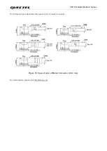
Страница 65: ...sed for antenna connection it is recommended to use U FL R SMT connector provided by Hirose Figure 33 Dimensions of U FL R SMT Connector Unit mm U FL LP serial connectors listed in the following figure can be used to match the U FL R SMT Figure 34 Mechanicals of U FL LP Connectors ...

Страница 66: ...LTE Standard Module Series The following figure describes the space factor of mated connector Figure 35 Space Factor of Mated Connector Unit mm For more details please visit http hirose com ...

Страница 67: ...ly and voltage on digital and analog pins of the module are listed in the following table Table 34 Absolute Maximum Ratings Parameter Min Max Unit VBAT_RF VBAT_BB 0 3 5 5 V USB_VBUS 0 3 5 5 V Peak Current of VBAT_BB 0 8 A Peak Current of VBAT_RF 1 8 A Voltage on Digital Pins 0 3 2 3 V Voltage at ADC0 0 VBAT_BB V Voltage at ADC1 0 VBAT_BB V ...

Страница 68: ...T VBAT_BB and VBAT_RF The actual input voltages must stay between the minimum and maximum values 3 4 3 8 4 5 V Voltage drop during transmitting burst Maximum power control level at EGSM 900 0 0 400 mV IVBAT Peak supply current during transmission slot Maximum power control level at EGSM 900 1 8 2 0 A USB_VBUS USB connection detection 3 0 5 0 5 25 V ...

Страница 69: ...900 DRX 9 USB disconnected 1 14 mA DCS1800 DRX 2 USB disconnected 1 70 mA DCS1800 DRX 5 USB disconnected 1 26 mA DCS1800 DRX 5 USB suspend 1 41 mA DCS1800 DRX 9 USB disconnected 1 13 mA WCDMA PF 64 USB disconnected 2 37 mA WCDMA PF 64 USB suspend 2 53 mA WCDMA PF 128 USB disconnected 1 66 mA WCDMA PF 256 USB disconnected 1 31 mA WCDMA PF 512 USB disconnected 1 14 mA LTE FDD PF 32 USB disconnected ...

Страница 70: ...USB connected 37 15 mA LTE FDD PF 64 USB disconnected 20 52 mA LTE FDD PF 64 USB connected 36 69 mA LTE TDD PF 64 USB disconnected 20 51 mA LTE TDD PF 64 USB connected 36 66 mA GPRS data transfer EGSM900 4DL 1UL 32 34 dBm 197 6 mA EGSM900 3DL 2UL 32 31 dBm 364 8 mA EGSM900 2DL 3UL 31 08 dBm 468 8 mA EGSM900 1DL 4UL 29 28 dBm 523 2 mA DCS1800 4DL 1UL 29 65 dBm 134 3 mA DCS1800 3DL 2UL 29 58 dBm 242...

Страница 71: ... 72 mA WCDMA B5 HSUPA 20 02 dBm 405 29 mA WCDMA B8 HSUPA 21 03 dBm 451 78 mA LTE data transfer LTE FDD B1 22 78 dBm 563 82 mA LTE FDD B3 23 39 dBm 583 24 mA LTE FDD B5 23 19 dBm 530 15 mA LTE FDD B8 23 87 dBm 578 26 mA LTE TDD B34 22 83 dBm 228 47 mA LTE TDD B38 23 55 dBm 357 07 mA LTE TDD B39 23 09 dBm 236 27 mA LTE TDD B40 23 19 dBm 333 39 mA LTE TDD B41 23 44 dBm 381 70 mA GSM voice call EGSM90...

Страница 72: ... mA EGSM900 DRX 5 USB suspend TBD mA EGSM900 DRX 9 USB disconnected 1 28 mA DCS1800 DRX 2 USB disconnected 1 66 mA DCS1800 DRX 5 USB disconnected 1 30 mA DCS1800 DRX 5 USB suspend TBD mA DCS1800 DRX 9 USB disconnected 1 19 mA WCDMA PF 64 USB disconnected 2 30 mA WCDMA PF 64 USB suspend TBD mA WCDMA PF 128 USB disconnected 2 29 mA WCDMA PF 256 USB disconnected 1 67 mA WCDMA PF 512 USB disconnected ...

Страница 73: ...d 14 55 mA WCDMA PF 64 USB connected 39 48 mA LTE FDD PF 64 USB disconnected TBD mA LTE FDD PF 64 USB connected TBD mA LTE TDD PF 64 USB disconnected TBD mA LTE TDD PF 64 USB connected TBD mA GPRS data transfer GSM850 4DL 1UL 31 77 dBm 231 mA GSM850 3DL 2UL 31 79 dBm 389 mA GSM850 2DL 3UL 30 80 dBm 497 mA GSM850 1DL 4UL 29 19 dBm 548 mA EGSM900 4DL 1UL 31 61 dBm 189 mA EGSM900 3DL 2UL 31 59 dBm 35...

Страница 74: ...GSM900 4DL 1UL 26 74 dBm 136 mA EGSM900 3DL 2UL 24 71 dBm 223 mA EGSM900 2DL 3UL 22 57 dBm 288 mA EGSM900 1DL 4UL 20 29 dBm 351 mA DCS1800 4DL 1UL 25 81 dBm 122 mA DCS1800 3DL 2UL 24 29 dBm 211 mA DCS1800 2DL 3UL 22 24 dBm 282 mA DCS1800 1DL 4UL 19 89 dBm 354 mA PCS1900 4DL 1UL 25 93 dBm 121 mA PCS1900 3DL 2UL 24 34 dBm 207 mA PCS1900 2DL 3UL 22 31 dBm 280 mA PCS1900 1DL 4UL 20 09 dBm 354 mA WCDMA...

Страница 75: ... 82 dBm TBD mA LTE FDD B8 22 80 dBm TBD mA LTE TDD B34 23 00 dBm TBD mA LTE TDD B38 22 45 dBm TBD mA LTE TDD B39 23 05 dBm TBD mA LTE TDD B40 23 02 dBm TBD mA LTE TDD B41 23 35 dBm TBD mA GSM voice call EGSM900 PCL 5 31 55 dBm 234 mA EGSM900 PCL 12 18 87 dBm 111 mA EGSM900 PCL 19 5 58 dBm 81 mA DCS1800 PCL 0 28 50 dBm 183 mA DCS1800 PCL 7 15 62 dBm 97 mA DCS1800 PCL 15 0 32 dBm 77 mA WCDMA voice c...

Страница 76: ...S1800 DRX 5 USB disconnected 1 11 mA DCS1800 DRX 5 USB suspend 1 28 mA DCS1800 DRX 9 USB disconnected 1 00 mA WCDMA PF 64 USB disconnected 2 11 mA WCDMA PF 64 USB suspend 2 25 mA WCDMA PF 128 USB disconnected 1 47 mA WCDMA PF 256 USB disconnected 1 15 mA WCDMA PF 512 USB disconnected 0 99 mA LTE FDD PF 32 USB disconnected 1 85 mA LTE FDD PF 64 USB disconnected 1 28 mA LTE FDD PF 64 USB suspend 1 4...

Страница 77: ...A LTE TDD PF 64 USB disconnected 18 29 mA LTE TDD PF 64 USB connected 33 10 mA GPRS data transfer EGSM900 4DL 1UL 32 44 dBm 199 mA EGSM900 3DL 2UL 32 39 dBm 372 mA EGSM900 2DL 3UL 31 23 dBm 478 mA EGSM900 1DL 4UL 29 53 dBm 533 mA DCS1800 4DL 1UL 29 77 dBm 136 mA DCS1800 3DL 2UL 29 65 dBm 244 mA DCS1800 2DL 3UL 28 31 dBm 293 mA DCS1800 1DL 4UL 26 40 dBm 309 mA EDGE data transfer EGSM900 4DL 1UL 27 ...

Страница 78: ...ransfer LTE FDD B1 23 61 dBm 607 mA LTE FDD B3 23 71 dBm 636 mA LTE FDD B5 23 70 dBm 568 mA LTE FDD B7 23 56 dBm 813 mA LTE FDD B8 24 11 dBm 591 mA LTE FDD B20 23 20 dBm 592 mA LTE FDD B28 23 77 dBm 559 mA LTE TDD B38 18 12 dBm 230 mA LTE TDD B40 18 68 dBm 233 mA LTE TDD B41 19 18 dBm 242 mA GSM voice call EGSM900 PCL 5 32 34 dBm 206 mA EGSM900 PCL 12 19 11 dBm 76 mA EGSM900 PCL 19 6 05 dBm 48 mA ...

Страница 79: ...ion Min Max Unit VIH Input high voltage 1 2 2 0 V VIL Input low voltage 0 3 0 6 V VOH Output high voltage 1 35 1 8 V VOL Output low voltage 0 3 0 45 V Parameter Description Min Max Unit USIM_VDD Power supply 1 7 1 9 V VIH Input high voltage 1 2 2 0 V VIL Input low voltage 0 3 0 6 V VOH Output high voltage 1 35 1 8 V VOL Output low voltage 0 3 0 45 V Parameter Description Min Max Unit USIM_VDD Powe...

Страница 80: ...bly and testing of the module adding ESD protective component to the ESD sensitive interfaces and points in the product design of the module ESD characteristics of the module s pins are as follows Table 40 Electrostatics Discharge Characteristics 25 C 45 Relative Humidity VIL Input low voltage 0 3 1 0 V VOH Output high voltage 2 55 3 0 V VOL Output low voltage 0 3 0 45 V Tested Interfaces Contact ...

Страница 81: ...ions such as voice SMS data transmission etc without any unrecoverable malfunction Radio spectrum and radio network are not influenced while one or more specifications such as Pout may exceed the specified tolerances of 3GPP When the temperature returns to the operating temperature range the module meets 3GPP specifications again Parameter Min Typ Max Unit Operating Temperature Range 3 35 25 75 C ...

Страница 82: ... This chapter describes the mechanical dimensions of the module All dimensions are measured in millimeter mm and the dimensional tolerances are 0 2 mm unless otherwise specified 7 1 Mechanical Dimensions Figure 36 Module Top and Side Dimensions Unit mm ...

Страница 83: ...LTE Standard Module Series Figure 37 Module Bottom Dimensions View Unit mm The flatness of EC200A series module of Remote Communication meets the requirements of JEITA ED 7306 standard NOTE ...

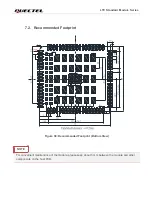
Страница 84: ...rd Module Series 7 2 Recommended Footprint Figure 38 Recommended Footprint Bottom View For convenient maintenance of the module please keep about 3 mm between the module and other components on the host PCB NOTE ...

Страница 85: ...dard Module Series 7 3 Top and Bottom Views Figure 39 Top and Bottom View of the Module These are renderings of the module For authentic appearance please refer to the module that you receive from Quectel NOTE ...

Страница 86: ...ity is less than 10 e g a drying cabinet 4 The module should be pre baked to avoid blistering cracks and inner layer separation in PCB under the following circumstances The module is not stored in Recommended Storage Condition Violation of the third requirement above occurs Vacuum sealed packaging is broken or the packaging has been removed for over 24 hours Before module repairing 5 If needed the...

Страница 87: ...den 2 Take out the module from the package and put it on high temperature resistant fixtures before baking All modules must be soldered to PCB within 24 hours after the baking otherwise put them in the drying oven If shorter baking time is desired see IPC JEDEC J STD 033 for the baking procedure 3 Pay attention to ESD protection such as wearing anti static gloves when touching the modules NOTE ...

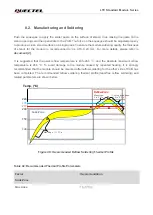
Страница 88: ...hat the peak reflow temperature is 235 246 C and the absolute maximum reflow temperature is 246 C To avoid damage to the module caused by repeated heating it is strongly recommended that the module should be mounted after reflow soldering for the other side of PCB has been completed The recommended reflow soldering thermal profile lead free reflow soldering and related parameters are shown below T...

Страница 89: ...e any coating material that may chemically react with the PCB or shielding cover and prevent the coating material from flowing into the module 4 Avoid using ultrasonic technology for module cleaning since it can damage crystals inside the module 5 Due to the complexity of the SMT process please contact Quectel Technical Supports in advance for any situation that you are not sure about or any proce...

Страница 90: ...ule Series Figure 41 Carrier Tape Dimension Drawing Table 43 Carrier Tape Dimension Table Unit mm 8 3 2 Plastic Reel Figure 42 Plastic Reel Dimension Drawing W P T A0 B0 K0 K1 F E 44 44 0 35 32 5 29 5 3 0 3 8 20 2 1 75 ...

Страница 91: ...ver tape to cover them then wind the heat sealed carrier tape to the plastic reel and use the protective tape for protection One plastic reel can load 250 modules Place the packaged plastic reel humidity indicator card and desiccant bag into a vacuum bag then vacuumize it Place the vacuum packed plastic reel into a pizza box Put 4 pizza boxes into 1 carton and seal it One carton can pack 1000 modu...

Страница 92: ...s_Manual 3 Quectel_RF_Layout_Application_Note 4 Quectel_Module_Secondary_SMT_Application_Note Abbreviation Description AMR Adaptive Multi Rate BeiDou BeiDou Navigation Satellite System bps Bytes per second CDMA Code Division Multiple Access CS Coding Scheme CTS Clear To Send DRX Discontinuous Reception DTE Data Terminal Equipment EFR Enhanced Full Rate EGSM Enhanced GSM ESD Electrostatic Discharge...

Страница 93: ...obal System for Mobile Communications HR Half Rate HSDPA High Speed Downlink Packet Access HTTPS Hypertext Transfer Protocol Secure LGA Land Grid Array LTE Long Term Evolution MCS Modulation and Coding Scheme MMS Multimedia Messaging Service NTP Network Time Protocol PAP Password Authentication Protocol PCB Printed Circuit Board PCM Pulse Code Modulation PING Packet Internet Groper PPP Point to Po...

Страница 94: ...ime Division Duplexing UDP User Datagram Protocol UMTS Universal Mobile Telecommunications System USB Universal Serial Bus U SIM Universal Subscriber Identity Module Vmax Maximum Voltage Value Vnom Nominal Voltage Value Vmin Minimum Voltage Value VIHmax Maximum Input High Level Voltage Value VIHmin Minimum Input High Level Voltage Value VILmax Maximum Input Low Level Voltage Value VILmin Minimum I...

Страница 95: ...es should be transmitting and the evaluation should confirm that the module s intentional emissions are compliant i e fundamental and out of band emissions The host manufacturer must verify that there are no additional unintentional emissions other than what is permitted in Part 15 Subpart B or emissions are complaint with the transmitter s rule s The Grantee will provide guidance to the host manu...

Страница 96: ...harmful interference and 2 this device must accept any interference received including interference that may cause undesired operation This equipment has been tested and found to comply with the limits for a Class B digital device pursuant to Part 15 of the FCC Rules These limits are designed to provide reasonable protection against harmful interference in a residential installation This equipment...

Страница 97: ... FCC regulations limiting both maximum RF output power and human exposure to RF radiation maximum antenna gain including cable loss must not exceed SM850 WCDMA Band5 LTE Band 5 7 0dBi GSM1900 WCDMA Band2 LTE Band 2 8 0dBi WCDMA Band 4 LTE Band 4 LTE Band 66 5 0dBi LTE Band 7 8 0dBi Radiation Exposure Statement This equipment complies with FCC radiation exposure limits set forth for an uncontrolled...

Отзывы: