Chapter 3 System Configuration
SP-7165/SP-7167 SERIES USER MANUAL
Page: 3-15
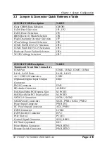
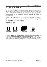
3.3 Jumper & Connector Quick Reference Table
CONNECTOR Description
NAME
Clear CMOS Data Selection
CMOS1
LVDS Panel Selection
JP1, JP2
LVDS Power Selection
JP3
BIOS Recovery Mode Selection
JP4
Flash Descriptor Override Selection
JP7
CFast Voltage Control Selection
JP9
COM1 Pin9 RI/5V/12V Selection
JP12
COM2 Pin18 RI/5V/12V Selection
JP15
Hardware Power Failure Selection
JP16
VCCIO Voltage Selection
JP17
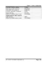
CONNECTOR Description
NAME
Mainboard Front Side Connectors
COM Port
COM1, COM2, COM3, COM4
LAN1, LAN2 Ports
LAN1, LAN2
4 x 1 USB 3.0 Connectors
USB1
(Optional) Digital Input/ Output
Connector
DIO1
DVI-I Connector
DVI1
HD Audio Connector
AUDIO1
Full-Sized Mini PCI Express Slot
M_PCIE1
Half-Sized Mini PCI Express Slot
M_PCIE2
SATA 3.0 Connectors
SATA1, SATA2
SATA Power Connectors
SATA_PWR1, SATA_PWR2
Power Input Connector
PWR_IN1
DC Power Input Connector
ATX_PWR1
LVDS Connector
LVDS1
LVDS Inverter Connector
INV1
PCIe Slot x4
PCI_E1
Control Signal Connector
SGN_BRD1
I2C Wafer (optional)
I2C1
Power Button Connector
PWR_BTN1
Remote Switch Connector
PWR_BTN2
Содержание SP-7165
Страница 9: ...vi Configuring WatchDog Timer B 25 Flash BIOS Update B 27 ...
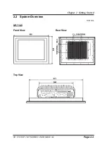
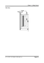
Страница 16: ...Chapter 2 Getting Started SP 7165 SP 7167 SERIES USER MANUAL Page 2 4 Side View ...
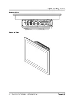
Страница 17: ...Chapter 2 Getting Started SP 7165 SP 7167 SERIES USER MANUAL Page 2 5 Bottom View Quarter View ...
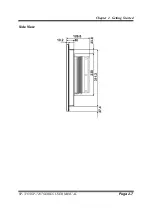
Страница 19: ...Chapter 2 Getting Started SP 7165 SP 7167 SERIES USER MANUAL Page 2 7 Side View ...
Страница 20: ...Chapter 2 Getting Started SP 7165 SP 7167 SERIES USER MANUAL Page 2 8 Bottom View Quarter View ...
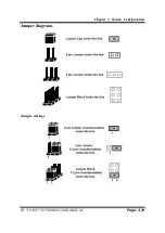
Страница 32: ...Chapter 3 System Configuration SP 7165 SP 7167 SERIES USER MANUAL Page 3 21 Jumper diagrams Jumper settings ...
Страница 151: ...Appendix B Technical Summary SP 7165 SP 7167 SERIES USER MANUAL Page B 2 System Block Diagram ...
Страница 177: ...Appendix B Technical Summary SP 7165 SP 7167 SERIES USER MANUAL Page B 28 ...

