


F
7/ 09
TOP100-4
9
by the boost inductance and parasitic
capacitance. R1 generates a pre-
compensation current proportional to
the instantaneous rectified AC input
voltage which directly varies the duty
cycle. C2 filters high frequency
switching currents while having no
filtering effect on the line frequency pre-
compensation current. R2 decouples
the pre-compensation current from the
large filter capacitor C3 to prevent an
averaging effect which would increase
total harmonic distortion. C1 filters
high frequency noise currents which
could cause errors in the pre-
compensation current.
General Circuit Operation (cont.)
When power is first applied, C3 charges
to typically 5.7 volts before TOPSwitch
starts. C3 then provides TOPSwitch
bias current until the output voltage
becomes regulated. When the output
voltage becomes regulated, series
connected Zener diodes VR1 and VR2
begin to conduct, drive current into the
TOPSwitch control pin, and directly
control the duty cycle. C3 together with
R3 perform low pass filtering on the
feedback signal to prevent output line
frequency ripple voltage from varying
the duty cycle. For more information,
refer to Design Note DN-7.
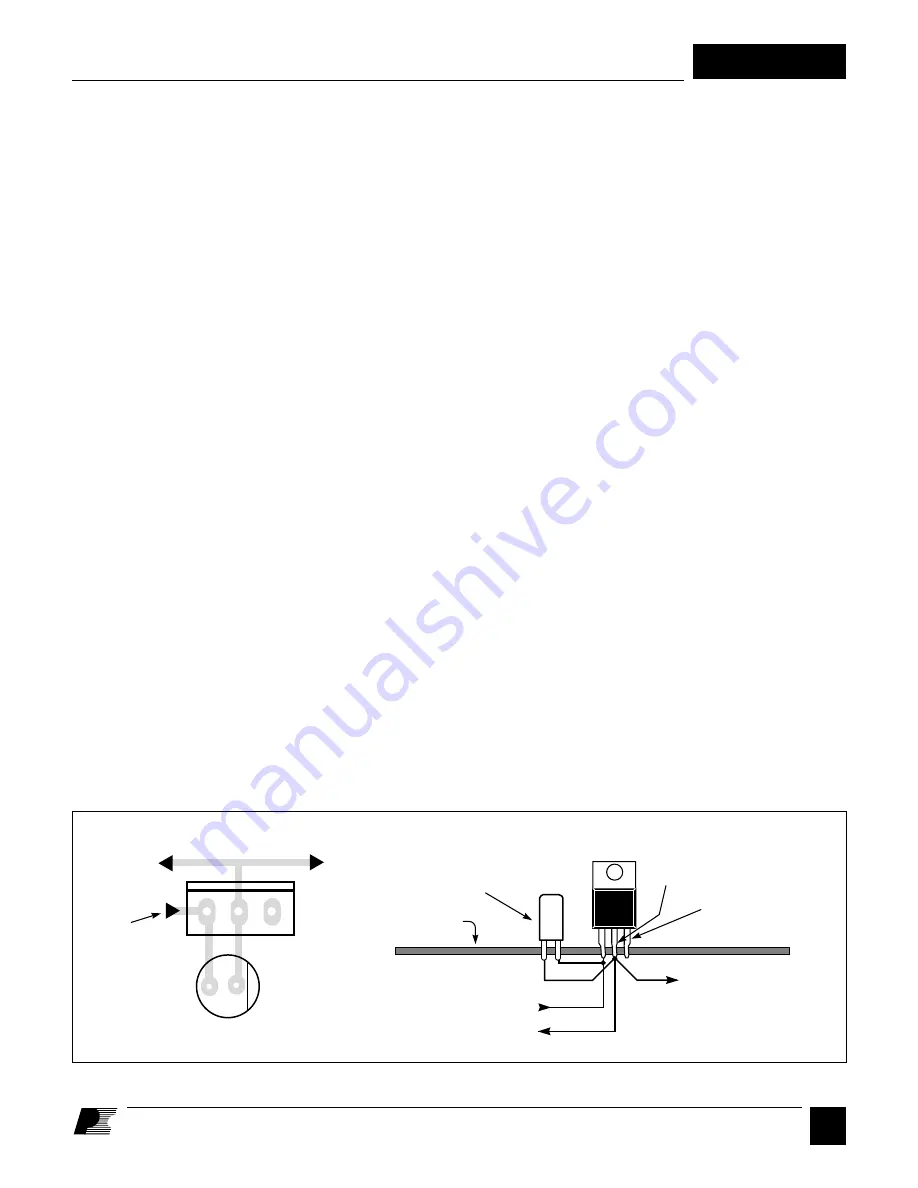
Keep the SOURCE pin length very short.
Use a Kelvin connection to the SOURCE
pin for the CONTROL pin bypass
capacitor. Use single point grounding
techniques at the SOURCE pin as shown
in Figure 11.
Minimize peak voltage and ringing on
the DRAIN voltage at turn-off. Use a
Zener or TVS Zener diode to clamp the
DRAIN voltage.
Do not plug the TOPSwitch device into
a “hot” IC socket during test. External
CONTROL pin capacitance may deliver
a surge current sufficient to trigger the
shutdown latch which turns the
TOPSwitch off.
Under some conditions, externally
provided bias or supply current driven
into the CONTROL pin can hold the
TOPSwitch in one of the 8 auto-restart
cycles indefinitely and prevent starting.
Shorting the CONTROL pin to the
SOURCE pin will reset the TOPSwitch.
To avoid this problem when doing bench
evaluations, it is recommended that the
V
C
power supply be turned on before the
DRAIN voltage is applied.
CONTROL pin currents during auto-
restart operation are much lower at low
input voltages (< 20 V) which increases
the auto-restart cycle period (see the I
C
vs. Drain Voltage Characteristic curve).
Short interruptions of AC power may
cause TOPSwitch to enter the 8-count
auto-restart cycle before starting again.
This is because the input energy storage
capacitors are not completely discharged
and the CONTROL pin capacitance has
not discharged below the pin internal
power-up reset voltage.
In some cases, minimum loading may
be necessary to keep a lightly loaded or
unloaded output voltage within the
desired range due to the minimum ON-
time.
For additional applications information
regarding the TOPSwitch family, refer
to AN-14.
Key Application Issues
Figure 11. Recommended TOPSwitch Layout.
PI-1240-110194
PC Board
Kelvin-connected
bypass capacitor
and/or compensation network
Bias/Feedback Input
Bias/Feedback Return
High-voltage Return
Bend DRAIN pin
forward if needed
for creepage
DRAIN
SOURCE
CONTROL
Do not bend SOURCE pin
Keep it short
High Voltage
Return
Bias/Feedback
Return
Bypass
Capacitor
D
S
C
TOP VIEW
Bias/Feedback
Input
Boost PFC Pre-regulator
TOPSwitch can also be used as a fixed
frequency, discontinuous mode boost
pre-regulator to improve Power Factor
and reduce Total Harmonic Distortion
(THD) for applications such as power
supplies and electronic ballasts. The
circuit shown in Figure 10 operates from
110 VAC and delivers 60 W at 265 VDC
with typical Power Factor over 0.99 and
THD of 5%. Bridge Rectifier BR1 full
wave rectifies the AC input voltage. L1,
D1, C4, and TOPSwitch make up the
boost power stage. D2 prevents reverse
current through the TOPSwitch body
diode due to ringing voltages generated