


2.3
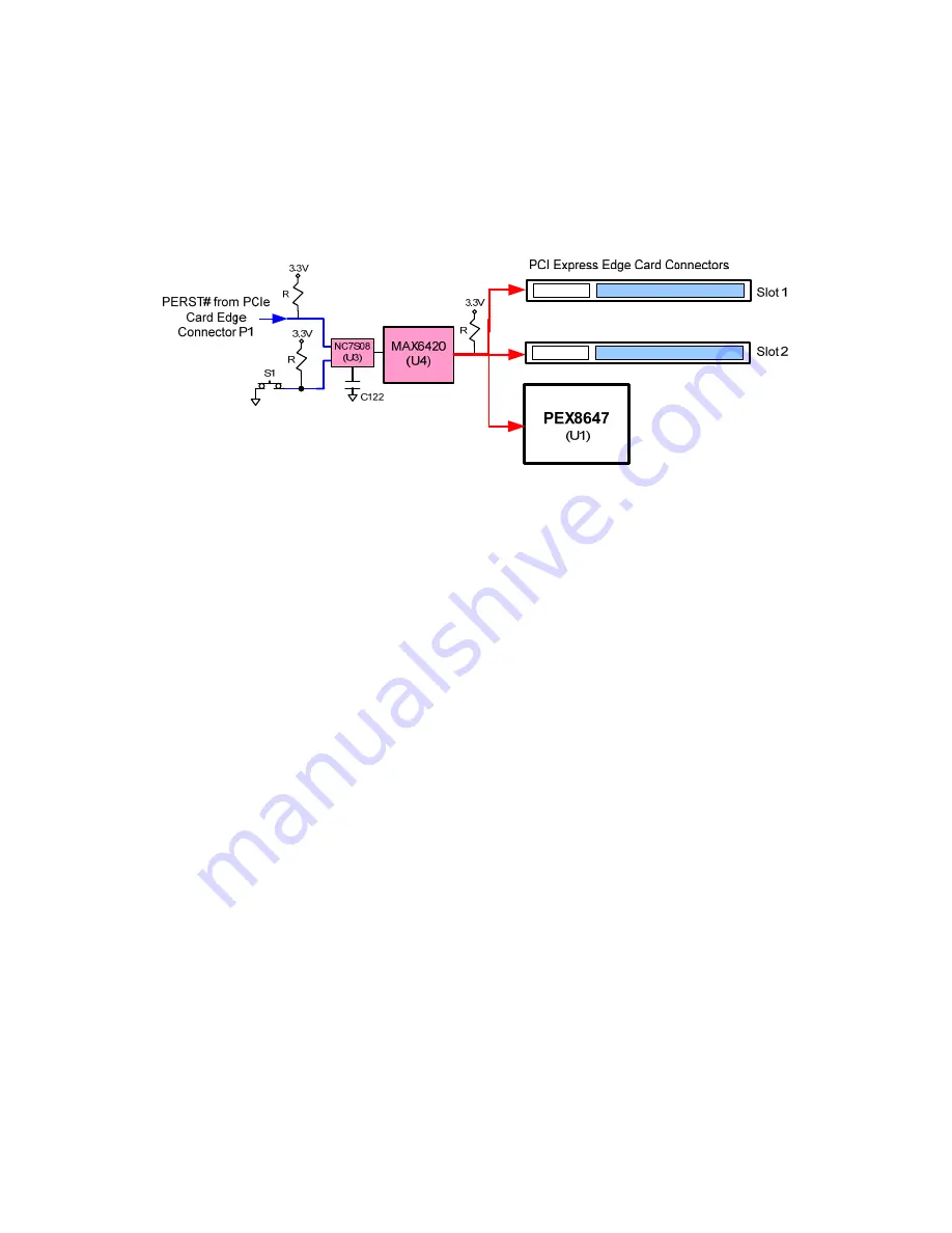
Reset Circuitry
The PEX 8647-AA RDK reset circuitry includes a MAX6420 adjustable reset timer (U4) and manual reset push-
button switch (S1). The reset timer accepts PERST# from the card edge (P1) and from S1 (logical-OR via U3).
The MAX6420 has the capability of adjusting the reset timeout period by changing the value of C122 (0.001
μ
F
≈
Figure 2-4. PEX 8647-AA RDK Reset Circuit
2.4
Serial EEPROM
The PEX 8647-AA RDK contains an 8-pin DIP socket for a serial EEPROM (U9). The board is populated with a
blank Atmel AT25256A 32-Kbit device. The AT25256A device can directly interface to the PEX 8647. When
programmed correctly, the serial EEPROM can be used to change the default configuration of the PEX 8647. A
blank EEPROM results in the default register values set in the PEX 8647. Please refer to the Software
Development Kit (SDK) documentation for additional information on how to program the serial EEPROM.
2.5
I
2
C Interface
The PEX 8647 implements an I
2
C slave interface, which allows an external I
2
C master to read and write device
registers through an out-of-band mechanism. The PEX 8647 I
2
C interface is accessible via a 7-bit address, at
data rates from 100 Kbps up to 3.4 Mbps. The RDK provides a dipswitch (SW2) to set the lower three bit I
2
C
address, I2C_ADD[2:0], of PEX 8647 and two cascaded 2x2, 0.1” pitch headers (JP9 and JP10), which interface
to the PEX 8647’s I
2
C port. This allows for cascading multiple RDKs together using standard ribbon cable, or
connecting various 3
rd
party I
2
C test equipment such as the Total Phase Aardvark I
2
C controller. (See
for pin assignments of JP9 and JP10).
2.6
Power Distribution
The PEX 8647-AA RDK has two sources for DC power. The first source is the card edge connector (P1). The x16
connector provides up to 5.5A at 12V and 3.0A at 3.3V. Card edge power is intended to power only RDK board
components. The dc/dc converter U7 converts 12V from the Card Edge connector to 1.0VCC to support the
SerDes and core power for the PEX 8647. The LDO (U8) converts 3.3V to 2.5VCC to support the IO power for the
PEX 8647. A 2-pin header (JP7) is used to measure the 2.5V current to the PEX 8647.
The second source includes two ATX HD power connectors, J2 and J3, and a 5V to 3.3V step down dc/dc
converter U6. J2 and J3 directly provide 12VCC up to 5.5A to each of PCI Express Edge Card Connectors
SLOT 1 and SLOT 2. The J2 and J3 also provide enough 5V power for the dc/dc converter (U6) to generate
3.3VCC up to 3A for each of SLOT 1 and SLOT 2. In other words, the second power source provides up to 150W
of power to SLOT 1 and SLOT 2 for high power graphic cards application. (See
for details).
PEX 8647-AA RDK Hardware Reference Manual, Version 1.2
8
Copyright © 2008 by PLX Technology, Inc. All rights reserved


