EL320.256-FD7 Operations Manual (020-0353-00A)
5
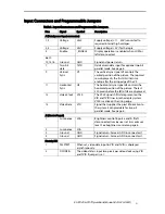
Input Connectors and Programmable Jumpers
Table1. Input Connectors and Programmable Jumpers.
Pins Signal Symbol Description
J1(Data/power input connector)
1, 2
Voltage
Vcc2
Supply voltage (+11…30V) converted to
required internal high voltages.
3, 4
Voltage
Vcc1
Supply voltage (+5 V) for the logic.
5
Enable
_ENABLE
Display operation is enabled when LOW or
left disconnected.
6,8,10
12,14,16
Ground
GND
Signal and power return.
7 Two-bit
data
TVID
Odd column data input for optional two bit
parallel mode. See page 6.
9 Vertical
Sync
VS
The vertical sync signal VS controls the
vertical position of the picture. The topmost
row displayed is the first HS HIGH time
ending after the rising edge of the VS.
11 Horizontal
Sync
HS
The horizontal sync signal HS controls the
horizontal position of the picture. The last
320 pixels before the fall of HS are displayed.
13
Video Clock
VCLK
The VCLK signal shifts data present on the
VID and TVID lines into the display system.
VCLK is active on the rising edge.
15
Video Data
VID
Signal that supplies the pixel information to
the system. Even pixel data for two pit
parallel mode. See page 6.
J2 (Control input)
1
Luminance
LCb
Brightness control inputs a and b. If left
disconnected, luminance is at its maximum
level. See brightness control on page 6.
2 Luminance
LCb
3
Ground
GND
Signal return. Same as GND in connector J1.
4
Ground
GND
Signal return. Same as GND in connector J1.
Pinstrip PS1
1
SELFTEST
When set, video data input in VID and TVID is displayed
asynchronously.
2
DCONFIG
The video data is input two pixels per video clock using VID
and TVID if jumper is set.


