background image

3

X-RSM400DV

5

6

7

8

5

6

7

8

A

B

C

D

E

F

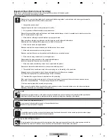
[Important Check Points for Good Servicing]

In this manual, procedures that must be performed during repairs are marked with the below symbol.
Please be sure to confirm and follow these procedures.

1. Product safety

Please conform to product regulations (such as safety and radiation regulations), and maintain a safe servicing environment by 
following the safety instructions described in this manual.

 Use specified parts for repair.

Use genuine parts.  Be sure to use important parts for safety.

  Do not perform modifications without proper instructions.

Please follow the specified safety methods when modification(addition/change of parts)  is required due to interferences such as 
radio/TV interference and foreign noise.

  Make sure the soldering of repaired locations is properly performed.

When you solder while repairing, please be sure that there are no cold solder and other debris.
Soldering should be finished with the proper quantity. (Refer to the example)

  Make sure the screws are tightly fastened.

Please be sure that all screws are fastened, and that there are no loose screws.

  Make sure each connectors are correctly inserted.

Please be sure that all connectors are inserted, and that there are no imperfect insertion.

  Make sure the wiring cables are set to their original state.

Please replace the wiring and cables to the original state after repairs.
In addition, be sure that there are no pinched wires, etc.

  Make sure screws and soldering scraps do not remain inside the product.

Please check that neither solder debris nor screws remain inside the product.

  There should be no semi-broken wires, scratches, melting, etc. on the coating of the power cord.

Damaged power cords may lead to fire accidents, so please be sure that there are no damages.
If you find a damaged power cord, please exchange it with a suitable one.

 There should be no spark traces or similar marks on the power plug.

When spark traces or similar marks are found on the power supply plug, please check the connection and advise on secure 
connections and suitable usage.   Please exchange the power cord if necessary.

a

  Safe environment should be secured during servicing.

When you perform repairs, please pay attention to static electricity, furniture, household articles, etc. in order to prevent injuries.  
Please pay attention to your surroundings and repair safely. 

2. Adjustments

To keep the original performance of the products, optimum adjustments and confirmation of characteristics within specification.
Adjustments should be performed in accordance with the procedures/instructions described in this manual.

4. Cleaning

For parts that require cleaning, such as optical pickups, tape deck heads, lenses and mirrors used in projection monitors, proper 
cleaning should be performed to restore their performances.

3. Lubricants, Glues, and Replacement parts

Use grease and adhesives that are equal to the specified substance. 
Make sure the proper amount is applied.

5. Shipping mode and Shipping screws

To protect products from damages or failures during transit, the shipping mode should be set or the shipping screws should be 
installed before shipment.  Please be sure to follow this method especially if it is specified in this manual.

Содержание x-rsm400dvh

Страница 1: ...01 Singapore 159936 PIONEER CORPORATION 2009 2009 Printed in Japan X RSM400DV RRV4011 DVD MINI COMPONENT SYSTEM X RSM400DV THIS MANUAL IS APPLICABLE TO THE FOLLOWING MODEL S AND TYPE S Model Type Power Requirement DVD Region No Serial No Remarks X RSM400DV LXCN AC 110 V to 240 V 3 LE LE ASEAN X RSM400DV DXCN AC 110 V to 240 V 4 ME ME LATIN AMERICA X RSM400DV DXCNRI AC 110 V to 240 V 2 RB RB MIDDLE...

Страница 2: ... 4 A B C D E F 1 2 3 4 For DVD Wave Length 656 nm Operating output 0 1 mW CW Class 1 Maximum output Class 1 For CD Wave Length 789 nm Operating output 0 15 mW CW Class 1 Maximum output Class 1 LASER DIODE CHARACTERISTICS ...

Страница 3: ... the product Please check that neither solder debris nor screws remain inside the product 8 There should be no semi broken wires scratches melting etc on the coating of the power cord Damaged power cords may lead to fire accidents so please be sure that there are no damages If you find a damaged power cord please exchange it with a suitable one 9 There should be no spark traces or similar marks on...

Страница 4: ...SECTION 5 DIAGNOSIS CONNECTION 5 1 1 1 ...

Страница 5: ...ser beams may damage the eyes Absolutely never permit laser beams to enter the eyes Also NEVER switch ON the power to the laser output part lens etc of the pick up if it is damaged 5 Cleaning the lens surface If there is dust on the lens surface the dust should be cleaned away by using an air bush such as used for camera lens The lens is held by a delicate spring When cleaning the lens surface the...

Страница 6: ...pair 1 Before replacing a component part first disconnect the power supply lead wire from the unit 2 All equipment measuring instruments and tools must be grounded d e d n u o r g d n a t e e h s e v i t c u d n o c a h t i w d e r e v o c e b d l u o h s h c n e b k r o w e h T 3 When removing the laser pick up from its conductive bag do not place the pick up on the bag This is because there is t...

Страница 7: ... 5 Do not use freon propelled chemicals These can generate electrical charges sufficient to damage ESD devices 6 Do not remove a replacement ESD device from its protective package until immediately before you are ready to install it Most replacement ESD devices are packaged with leads electrically shorted together by conductive foam aluminum foil or comparable conductive materials 7 Immediately be...

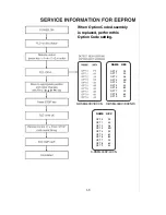
Страница 8: ...5 09 OPT 6 83 OPT 7 20 OPT 8 60 OPT 9 00 NAME HEX OPT 0 F5 OPT 1 00 OPT 2 A4 OPT 3 BD OPT 4 00 OPT 5 69 OPT 6 83 OPT 7 20 OPT 8 60 OPT 9 00 X RSM400DV DXCN X RSM400DV DXCNRI X RSM400DV LXCN When Option Code Assembly is replaced perform this Option Code setting ...

Страница 9: ... the following steps 1 When the USB device is inserted at the USB function the screen is changed into downloading screen 2 When downloading is completed the message Completed is displayed at the top left on the screen 3 Turn on the power press the SETUP button of the remote controller on the USB FUCTION When the SETUP window is displayed on the screen move down once to select the DISPLAY menu Go t...

Страница 10: ...sions WxHxD 273 x 336 x 372 mm Operating temperature 5 C to 35 C Operating humidity 5 to 85 FM Tuning Range 87 5 108 0 MHz AM Tuning Range 530 1 700 KHz DXCN 531 1 602 KHz LXCN DXCNRI Output Power Front 110 W x 2 Sub Woofer 180 W 0 1 D H T Frequency Response 42 20000 Hz Signal to noise ratio 75 dB F F REW Time 120 sec C 60 Frequency Response 250 8000 Hz Signal to Noise Ratio 43 dB Channel Separati...

Страница 11: ...1 8 ...

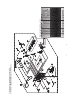
Страница 12: ...300 274 289 451 464 464 294 463 464 464 464 277 277 464 464 454 A00 A43 A42 CABLE5 MAIN MIC SMPS 275 A B C D C M B N F N H P H G I O A41 DVD I A26 J K M L E CABLE4 CABLE6 CABLE1 CABLE2 CABLE7 CABLE8 E U F 464 292 290 291 455 O CABLE3 Q R T S U FRONT USB 464 464 267 271 263 265 258 263 250 464 464 268 264 257 253 256 253 252 251 256 270L 272A 272C 272D 272B 269 270R SECTION 2 EXPLODED VIEWS 2 1 2 2...

Страница 13: ...ME MCT404 LENS VOL 259 MEY61851201 Knob MOLD ABS MP 211 HOME MCT404 MO 260 EAX61426702 PCB 1 MDT404 MCT404 JACK FR 1 1 1 263 4901R 0002C Damper Assembly HOME HE902 NO 264 4974R 0041B Guide MOLD ABS HOME EJECT ASSY L MOL 265 4974R 0042B Guide MOLD ABS HOME EJECT ASSY R MOL 267 MHK61843101 Sheet PRESS PC 0 5 CDT 118 39 0 5 FL 268 MBG62154401 Button MOLD ABS HF 380 HOME MCT404 MO 269 MBG62154601 Butt...

Страница 14: ...k Mechanism Parts 50 093 41585 50 093 41585 PIGE 007 6768RZGP03A Deck Mechanism Parts 50 222 41226 PIGEON GEAR IDLER 008 6768R SP01F Deck Mechanism Parts 01 082 4598 PIGEON SPRING CWL4 009 6768R MP01C Deck Mechanism Parts 50 219 4014 PIGEON MOLD CWL44 011 6768R SP01A Deck Mechanism Parts 01 081 4601 PIGEON SPRING CWL4 013 6768RZSP02A Deck Mechanism Parts 01 082 4688 PIGEON SPRING 015 6768R AP01A D...

Страница 15: ...MP01C Deck Mechanism Parts 50 219 4014 PIGEON MOLD CWL44 011 6768R SP01A Deck Mechanism Parts 01 081 4601 PIGEON SPRING CWL4 013 6768RZSP02A Deck Mechanism Parts 01 082 4688 PIGEON SPRING 015 6768R AP01A Deck Mechanism Parts 50 268 3016 PIGEON ARM CWL44 016 6768RZGP04B Deck Mechanism Parts 50 093 31582 50 093 31582 PIGE 017 6768R AP01C Deck Mechanism Parts 50 239 4072 PIGEON ARM CWL44 018 6768R GP...

Страница 16: ...Motor Assembly DC RF 500TB AUDIO cdm h1703 MA 156 EBR60797401 PCB Assembly Deck 3 CHANGER CDM H1713 DVM H1713 159 MJS57233701 Tray MOLD ABS HF 380 DECK MECHA DVM 162 4400R 0012A Belt MOLD RUBBER DECK MECHA MAIN C 163 4470R 0190A Gear MOLD POM DECK MECHA PULLEY CD 164 4470RB0003A Gear MOLD POM HOME LOADING CDM H15 165 EBR48757901 PCB Assembly CDM H1703 main 166 4470RB0007A Gear MOLD POM HOME PU DOW...

Страница 17: ...NO DESCRIPTION SPECIFICATION REMARKS A60L EAB61030301 Speaker Assembly MCS404 049 01368 07 EAW MCS404 A60R EAB61030201 MCS404F 049 01368 07 EAW MCS40 2 11 A60R A60L 4 SPEAKER SECTION 1 FRONT SPEAKER Speaker Assembly ...

Страница 18: ...LOCA NO PART NO DESCRIPTION SPECIFICATION REMARKS A90 EAB61030401 Speaker Assembly MCS404W 049 01368 07 EAW MCS40 2 12 2 PASSIVE SUBWOOFER A90 ...

Страница 19: ...Speaker 803 Packing Main Set 803 Packing Main Set 804 Bag Main Set Remote Controller Box Front Speaker Bottom Instruction Ass y 803WT Packing Woofer Top 803FB Packing 803FT Packing Front Speaker Top 803WB Packing Woofer Bottom 802 900 801 Battery Antenna Loop AM Antenna T FM 811 RCA Cable 1Pin Black ...

Страница 20: ...3 1 5V 0AH NSP 811 6850R PAA8H Cable Assembly 061104 RCA PLUG 3 2 RCA PLUG 824 EAA56672101 Antenna Loop SN080113AM SINGLE 4DB 10UH HW 825 5010R T001D Antenna T T13021F 2 SINGLE 0DB 0OHM 0 1 REMOTE CONTROLLER S AL LOCA NO PART NO DESCRIPTION SPECIFICATION REMARKS 900 AKB72913811 Remote Controller Assembly CB1 MDT404 MINI DVD Pioneer CONTRAST TABLE X RSM400DV DXCN X RSM400DV DXCNRI and X RSM400DV LX...

Страница 21: ...2 12 ...

Страница 22: ...ine Check short of P9701 P9702 line NO Check short of P9701 line NO Replace IC901 902 YES Check the DC V of C905 if DC V is over 400V NO YES Check the DC V of C909 C903 C921 If DC V is in 14 19V and it is steady Check IC901 902 YES YES Check the DC V of C981 C945 If DC V is 6 1V YES Check the DC V of C950 C951 If DC V is in 34V YES OK SECTION 3 ELECTRICAL PART ...

Страница 23: ...K CHECK Check the pin3 of P9702 if DC V is over 28V YES OK OK OK NO Replace IC101 KIA7042 NO YES YES YES YES Check if IC101 of out put voltage is over 4 3V YES Check voltage of IC100 LC87Fxxx pin4 YES Refer to SMPS troubleshooting MICOM PART CHECK I NO Check P SENS P7904_pin6 NO Check both end voltage of IC101 KIA7042 Check If input voltage of IC101 is over 5V Check the periphery of IC101 KIA7042 ...

Страница 24: ...4MHz Check the operation Check P SENS P7904_pin6 Check both end voltage of D101 Check If output of D101 is 5V YES Check D101 MICOM PART CHECK II NO Replace D101 YES OK YES OK 6 IC103 S24CS16A01 PART CHECK YES YES YES YES pin93 DATA pin94 CLK Check MICOM NO Check MICOM voltage 5V CHECK IC100 PIN93 94 NO Replace MICOM NO Refer to MICOM troubleshooting OK OK ...

Страница 25: ...L 26 pin23 FL 22 pin22 VKK over 26V pin19 5 6V Check IC501 ET6315 voltage pin30 VKK 26V pin13 43 5V OK OK NO Replace IC501 NO If voltage is not 5V check input and output of L502 YES Check IC501 Check CN304 connection YES YES Check each pin voltage OK YES NO YES YES Check IC102 IC501 data communication 3pin 9pin STB 2pin 7pin DATA 4pin 8pin CLK OK NO Replace IC102 NO IC102 pin2 3 4 check data Input...

Страница 26: ...24 25 26 DATA input PWM wave Check PWM modulator output FL pin75 74 FD pin71 70 check other output Check IC604 PS9830 VDD pin voltage 3 10 22 29 39 47 56 65 72 87 94 check X601 pin2 3 3V OK Replace X601 NO YES Check X601 12 288MHz OK Refer to DVD troubleshooting NO Check P7403 DVD assy communication Check each line resistor output NO Check IC604 PS9830 DATA input Replace R671 R670 R665 NO YES Chec...

Страница 27: ... Check each line resistor output voltage NO YES Check each input IC700 pin22 23 44 12V Replace the coil NO YES Check output line coil POWER AMP PART CHECK OK YES Check each IC700 pin27 26 32 35 40 41 input voltage YES Check PWM modulator input each pin6 8 16 18 YES POWER output IC700 pin28 31 36 39 ...

Страница 28: ... P7501 pin6 L CH pin8 D CH Check IC801 MC4580 pin4 12V pin8 12V Check IC201 pin6 12V pin7 3 3V Refer to SMPS troubleshooting Check P201 connection Check IC501 ES8390 pin55 input data Check IC501 ES8390 output data Check CN202 pin4 5 5V pin11 12 3 3V Check IC201 pin13 RST pin11 MCLK pin9 DATA YES YES YES YES YES YES YES YES YES YES YES YES NO NO Check IC200 BU4052 pin7 12V pin16 12V Each function o...

Страница 29: ...head input IC201_pin34 37 Check IC201 HA12237 _pin16 12V input YES Check IC201_ pin5 26 output signal YES Check IC201 pin14 mute operation YES Check IC201 Check A B DECK head input TAPE PLAY PART CHECK NO Replace head wire and tape DECK mechanism NO Replace IC201 YES OK YES OK NO Check IC202_pin10 HIGH YES Check IC202 NO Replace IC202 YES OK ...

Страница 30: ... Check IC201_ pin10 21 output Check IC100_ pin23 HIGH TAPE REC PART CHECK NO Replace IC201 Replace IC202 YES OK NO Check L203_pin2 3 oscillation Check Q205 D1304 _ base HIGH NO Check IC202_pin4 HIGH YES OK OK YES YES YES YES YES Check IC201_pin7 24 record input YES Check P2203_pin5 3 input and pin8 erase input YES ...

Страница 31: ...201 YES Check DVD MD module YES POWER ON Does DVD CD appear at FLD YES YES Does no disc or time are appeared at FLD YES Check connector P7501 Check the voltage of each pin on P201 Does it appear DVD error at FLD Does AUX FM 87 5 AM USB appear at FLD Func Check connector P400 OK DVD ELECTRICAL TROUBLESHOOTING GUIDE POWER ON ...

Страница 32: ...M works properly Check the related circuit of ES8390 IC501 pin133 134 137 138 139 140 NO YES ES8390 VIDEO outputs properly NO Check the MD mecha NO Check the cable connection between DVD PCB and MD MECHA Does tray move inside when it is closed position YES YES OPEN_SW CLOSE_ SW Signals on P406 are ok Check the output signal of ES8390 to IC401 for control OPEN CLOSE NO YES OPEN CLOSE signals on IC4...

Страница 33: ...inner side when it is at outer position YES YES YES SLED signal is OK Check the MD NO YES Motor Driver DRV_MMUTE pin 3 High A NO Check Focus connection on ES8390 and motor driver IC NO Check cable connection with pick up head Optical lens is moving for searching focus YES YES Proper Focus outputs to motor driver Check the motor driver IC401 NO YES Proper F F outputs B ...

Страница 34: ...CDLD output properly Check the related circuit of laser power transistor NO YES Collector voltage of power transistor is ok Q405 Q406 Put disc in tray B NO Check the SPINDLE related circuit on ES8390 NO Check the cable connection between P400 and MD Does SPINDLE rotate YES YES YES Proper SPINDLE signal on ES8390 Check the SPINDLE control of motor driver IC401 NO SPIN SPIN output properly C Laser o...

Страница 35: ... C D from MD Check the related circuit of ES8390 FOCUS signal NO YES Proper FOD signal on IC401 NO Check the related circuit between IC401 and ES8390 NO Check cable connection on pick up head Tracking ok YES YES YES Proper TRD signal on IC401 Check the tracking control on motor driver IC401 NO T T output properly Check RF signal waveform NO Disc play C D ...

Страница 36: ... and CN201 NO YES Check the MAIN PCB All outputs are ok during playing disk YES YES Audio signal data on ES8390 is ok For example composite video Check the video mute TR Q507 ES8390 video signal data NO Picture signal data on ES8390 is ok D TEST END ...

Страница 37: ...201 NO Check the HRST signal Check Searching or USB Display YES YES Check the USB and DVD part YES Check the USB part supply CN205 NO Check the USB data line CN205 Check Reading OK YES YES Check the ES8390 Check DATA LINE pin98_USB_NO 99_PO YES TURN ON USB OK ...

Страница 38: ... 17 1 WHEN POWER ON RESET DATA ETC WAVEFORM WAVEFORMS OF MAJOR CHECK POINT SPI DI SPI DO TX LCS3 FLASH 1 2 3 4 IC501 pin 72 IC501 pin 46 IC501 pin 47 IC503 pin 1 HRST 5V D D 5 6 IC501 pin 91 IC501 pin 90 ...

Страница 39: ... 3 STARTING ACTION WAVEFORM IN MD DEVICE 4 FOCUS WAVEFORM AT CD SL Driver STBY SLEGN SL 11 12 IC401 pin 18 IC401 pin 17 F F 13 14 IC401 pin 3 IC401 pin 4 open UP sw DOWN sw close 7 8 9 10 IC401 pin 11 IC501 pin 63 IC501 pin 59 IC401 pin 10 ...

Страница 40: ...D 6 AT POWER ON SPINDLE SIGNAL AT MD DECK 7 TRACKING SIGNAL Q405 DVD_LD Q406 CD_LD 15 16 Q405 Q406 Sclavijad Sclavija Sclavija 17 18 19 IC401 pin 21 IC401 pin 15 IC401 pin 16 Tro Tr Tr 20 21 22 IC401 pin 7 P400 pin 16 P400 pin 17 ...

Страница 41: ...3 20 9 DISK TYPE JUGEMENT WAVEFORM 8 RF WAVEFORM DVD F FDO SVRRF 23 24 25 P400 pin 18 IC401 pin 6 IC401 pin 23 CD F FDO SVRRF 26 27 28 P400 pin 18 IC401 pin 6 IC401 pin 23 ...

Страница 42: ...3 21 WIRING DIAGRAM 3 DVD CHANGER MD SMPS DVD PCB MAIN PCB 15P 8P 5P 23P 11P 12P DOUBLE DECK MECHANISM 3P 8P 13P 18P FRONT PCB USB VOL PCB MIC PCB 4P 16P 3P 10P 36P 6P ...

Страница 43: ...UDIO MICOM AMP_PRT SD PDN PWM_RST DATA CLK S 24CS16A01 EEPROM EEPROM DATA CLK DVD_RST CS CLK DI DO 5345_RST CLK DATA TUNER DECK A DECK B HA12237F Cassette Deck ASP BU2090 EXPANDER K K K K K K K K DECK S W AUX BU4052 AUDIO S W SCLK SDIO SEN RST GAIO2 MAIN AUDIO IN 4052_A B TUNER AUX IN L R L R ERASE REC L R MIC S4308 USB H P D D MIC SIG FLT DISPLAY PT6324 FLT DRIVER VFD_STB DO CLK TAPE_A B HALL_A B...

Страница 44: ...CUS SLED SPINDLE TRACKING AMP_STBY SLED F T LOAD SPINDLE M DECK MECHANISM MOTOR DRIVE IC IP9011 MICOM I F SCI SDA DMA 0 11 DB 0 15 DSCK CKE CS0 RAS0 SPI_CS CLK DI KO PWM I F CE CLK DI DO MRST LRCK BCK ADATA 0 3 USBP USBN Aux IN TUNER AK5358A POWER I F 3 8V 12V 3 3V REG 3 3V 5V USB CON Component Composite Y G Pb B Pr R Composite MCLK BCK LRCK DATA MIC I F FRONT TAPE ...

Страница 45: ...3 24 ...

Страница 46: ...RIGINAL DESIGN BE MODIFIED OR ALTERED WITH OUT PERMISSION FROM THE PIONEER CORPORATION ALL COMPONENTS SHOULD BE REPLACED ONLY WITH TYPES IDENTICAL TO THOSE IN THE ORIGINAL CIRCUIT SPECIAL COMPONENTS ARE SHADED ON THE SCHEMATIC FOR EASY IDENTIFICATION THIS CIRCUIT DIAGRAM MAY OCCASIONALLY DIFFER FROM THE ACTUAL CIRCUIT USED THIS WAY IMPLEMENTATION OF THE LATEST SAFETY AND PERFORMANCE IMPROVEMENT CH...

Страница 47: ...A 1 2 3 4 5 6 7 8 9 10 11 12 B C D E F G H I J K L M N O P Q R S T 1 8 9 2 3 4 5 6 WAVEFORM 2 MPEG CIRCUIT DIAGRAM 3 27 3 28 ...

Страница 48: ...A 1 2 3 4 5 6 7 8 9 10 11 12 B C D E F G H I J K L M N O P Q R S T 11 17 25 28 12 18 19 13 14 23 26 24 27 22 21 15 16 20 7 10 WAVEFORM 3 30 3 SERVO CIRCUIT DIAGRAM 3 29 ...

Страница 49: ...A 1 2 3 4 5 6 7 8 9 10 11 12 B C D E F G H I J K L M N O P Q R S T 3 31 3 32 4 I O CIRCUIT DIAGRAM ...

Страница 50: ...A 1 2 3 4 5 6 7 8 9 10 11 12 B C D E F G H I J K L M N O P Q R S T 3 33 3 34 5 MICOM INTERFACE CIRCUIT DIAGRAM ...

Страница 51: ...A 1 2 3 4 5 6 7 8 9 10 11 12 B C D E F G H I J K L M N O P Q R S T 3 35 3 36 6 PWM CIRCUIT DIAGRAM ...

Страница 52: ...A 1 2 3 4 5 6 7 8 9 10 11 12 B C D E F G H I J K L M N O P Q R S T 3 37 3 38 7 AMP CIRCUIT DIAGRAM ...

Страница 53: ...A 1 2 3 4 5 6 7 8 9 10 11 12 B C D E F G H I J K L M N O P Q R S T 3 39 3 40 8 DECK CIRCUIT DIAGRAM ...

Страница 54: ...3 41 3 42 9 FRONT CIRCUIT DIAGRAM A 1 2 3 4 5 6 7 8 9 10 11 12 B C D E F G H I J K L M N O P Q R S T ...

Страница 55: ...3 43 3 44 10 USB VOLUME CIRCUIT DIAGRAM A 1 2 3 4 5 6 7 8 9 10 11 12 B C D E F G H I J K L M N O P Q R S T ...

Страница 56: ...3 45 3 46 11 MIC CIRCUIT DIAGRAM A 1 2 3 4 5 6 7 8 9 10 11 12 B C D E F G H I J K L M N O P Q R S T ...

Страница 57: ... EE Mode V IC 200 BU4052 1 0 01 2 0 01 3 0 01 4 0 01 5 0 01 6 0 01 7 6 29 8 0 01 9 0 01 10 0 01 11 0 01 12 0 01 13 0 01 14 0 01 15 0 01 16 5 96 IC801 MC4580 1 0 06 2 0 04 3 0 04 4 12 23 5 0 04 6 0 06 7 0 06 8 11 58 IC802 MC4580 1 0 01 2 0 01 3 0 03 4 11 28 5 0 03 6 0 02 7 0 01 8 11 26 IC103 M24C16 1 0 01 2 0 01 3 0 01 4 0 01 31 1 11 32 3 35 33 1 17 34 0 42 35 0 29 36 3 35 37 0 02 38 1 5 39 0 04 40...

Страница 58: ... 16 25 0 26 1 23 27 2 21 28 1 56 IC502 SDRAM 1 3 39 2 0 6 3 3 39 4 0 71 PIN NO PB Mode V 5 0 71 6 0 7 0 91 8 0 71 9 3 38 10 0 86 11 0 94 12 0 13 0 92 14 3 38 15 0 02 16 0 17 3 3 18 3 2 19 3 26 20 0 09 21 0 03 22 0 09 23 0 09 24 0 55 25 0 56 26 1 6 27 3 38 28 0 01 29 1 38 30 1 53 31 1 79 32 1 38 33 2 62 34 0 35 0 02 36 0 02 37 3 38 38 1 45 39 0 02 40 0 41 0 01 42 0 83 43 3 38 44 0 89 45 0 77 46 0 0...

Страница 59: ...3 51 3 52 PRINTED CIRCUIT BOARD DIARGAMS 1 1 MAIN P C BOARD DIAGRAM TOP VIEW ...

Страница 60: ...1 2 MAIN P C BOARD DIAGRAM BOTTOM VIEW 3 53 3 54 ...

Страница 61: ...3 55 3 56 2 1 DVD P C BOARD DIAGRAM TOP VIEW ...

Страница 62: ...2 2 DVD P C BOARD DIAGRAM BOTTOM VIEW 3 57 3 58 ...

Страница 63: ...3 59 3 60 3 SMPS P C BOARD DIAGRAM NOTE Warning Parts that are shaded are critical With respect to risk of fire or electrical shock ...

Страница 64: ...3 61 3 62 4 FRONT P C BOARD DIAGRAM 5 HEADPHONE P C BOARD DIAGRAM 6 MIC P C BOARD DIAGRAM 7 JACK P C BOARD DIAGRAM ...

Страница 65: ...3 63 3 64 ...

Страница 66: ...409BA TR Bipolar KTD1304S NPN 12V 25V 20V 300MA Q502 0TR130409BA TR Bipolar KTD1304S NPN 12V 25V 20V 300MA Q503 0TR130409BA TR Bipolar KTD1304S NPN 12V 25V 20V 300MA Q506 0TR129809BB TR Bipolar KTA1298Y PNP 5V 35V 30V 0 Q507 0TR130409BA TR Bipolar KTD1304S NPN 12V 25V 20V 300MA X501 EAW32919201 Crystal HC49SMD 27MHZ 27MHZ 20PPM 15pF A43 PCB Assembly Front A43 EBR64580201 PCB Assembly Front MDT404 ...

Страница 67: ... 12VDC 0 05A VE SW312 EBF40098801 Switch Tact SKRGAED010 1C1P 12VDC 0 05A VE SW313 EBF40098801 Switch Tact SKRGAED010 1C1P 12VDC 0 05A VE SW314 EBF40098801 Switch Tact SKRGAED010 1C1P 12VDC 0 05A VE SW315 EBF40098801 Switch Tact SKRGAED010 1C1P 12VDC 0 05A VE SW316 EBF40098801 Switch Tact SKRGAED010 1C1P 12VDC 0 05A VE SW317 EBF40098801 Switch Tact SKRGAED010 1C1P 12VDC 0 05A VE SW318 EBF40098801 ...

Страница 68: ...Z 450V SMPS TTL ASSY CABLE7 EAD42218201 Harness Single 15P 140MM XD123 GIL G GIL G CABLE8 EAD60517002 Harness Single HS LG08 006 A2507H02 08 A2507H BD901 EAH42986602 Diode Bridge RBU605M B C V50 600V 1 1V 2UA C902 EAE42617201 Capacitor Ceramic Radial CT7 Y10Y5U9E222MSEW 2200pF 20 C903 0CE1066K618 Capacitor AL Radial SMS5 0TP50VB10M 10uF 20 50V 7 C906 EAE42617701 Capacitor Ceramic Radial CT7 Y7Y5U9...

Страница 69: ...S CONNECTION When diagnosing Main Assembly or CD Total Assembly perform the following connection and style A26 Mechanism Assembly Extension FFC GGD1423 Connecting it between PCB Assembly DVD and Option Code Assembly 5 1 ...

Отзывы: