PDP-503PC
92
1
2
3
4
1
2
3
4
C
D
F
A
B
E
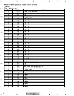
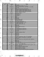
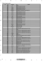
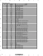
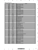
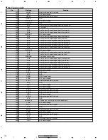
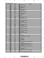
Pin Function (3/3)
No.
Pin Name
Function
101
P52
NC terminal
102
P53
NC terminal
103
AVCC
3.3V power supply
104
VREF
A/D, D/A reference voltage input (unused)
105
STOPB
The drive control input from IC1703 (PE5064)
106
P41
NC terminal
107
RYBY
The flash memory note ready input
108
ADR_K_EMG_L1
The emergency input from panel bottom address resonance block
109
ADR_K_EMG_U1
The emergency input from panel upper address resonance block
110
ADR_K_EMG_L2
The emergency input from panel bottom address resonance block (unused)
111
ADR_K_EMG_U2
The emergency input from panel upper address resonance block (unused)
112
P47
NC terminal
113
AVSS
GND
114
VSS
GND
115
MUTE_ADR
The panel mute signal input
116
MUTE_SUS
The X and Y drive mute signal output (unused)
117
P15
NC terminal
118
HD
The HD signal input from outside Assy (RGB Assy etc.)
119
P13
NC terminal
120
P12
NC terminal
121
PC_VIDEO
The PC/Video identification output
122
VD
The HD signal input from outside Assy (RGB Assy etc.)
123
MD0
The microcomputer mode of operation select signal input
124
MD1
The microcomputer mode of operation select signal input
125
MD2
The microcomputer mode of operation select signal input
126
PG0
NC terminal
127
CS_31Y
IC1301, IC1401 (PD6358) control signal
128
CS_31X
IC1301, IC1401 (PD6358) control signal


