A product of PHYTEC Technology Holding Company
L-827e.A3 phyCORE-i.MX 6UL/ULL Hardware
Manual
Страница 1: ...A product of PHYTEC Technology Holding Company L 827e A3 phyCORE i MX 6UL ULL Hardware Manual...
Страница 2: ...dware Manual PHYTEC Messtecknik GmbH 2 L 827e A3 phyCORE i Mx 6UL ULL Hardware Manual Document Title L 827e A3 phyCORE i Mx 6UL ULL Hardware Manual Article Number L 827e A3 Release Date 18 07 2022 SOM...
Страница 3: ...L 827e A3 phyCORE i MX 6UL ULL Hardware Manual PHYTEC Messtecknik GmbH 3...
Страница 4: ...re much of the value of the phyCORE module lies in its layout and test Production ready Board Support Packages BSPs and Design Services for our hardware will further reduce your development time and r...
Страница 5: ...pect to the pin header row connectors power connector and serial interface to a host PC 1 4 Product Change Management and Information Regarding Parts Populated on the SOM SBC With the purchase of a PH...
Страница 6: ...through the contact information given within this manual 1 5 PHYTEC Documentation PHYTEC will provide a variety of hardware and software documentation for all of our products This includes any or all...
Страница 7: ...ication Notes and Technical Notes These will be done on a case by case basis Most of the documentation can be found in the applicable download page of our products Tip After finishing the Quickstart G...
Страница 8: ...n this manual 0x41 complete address byte 0x83 to read from the device and 0x82 to write to the device Tables that describe jumper settings show the default position in bold blue text Text in blue indi...
Страница 9: ...C Output Open collector output without pull up requires an external pull up OC 5V Input PD 5 V tolerant input with pull down 5V_PD LVDS Input Differential line pairs 100 Ohm LVDS level input LVDS_I LV...
Страница 10: ...hyCORE i MX 6UL ULL Hardware Manual PHYTEC Messtecknik GmbH 10 PCIe Output Differential line pairs 100 Ohm PCIe level output PCIe_O MIPI CSI 2 Input Differential line pairs 100 Ohm MIPI CSI 2 level in...
Страница 11: ...used in reference to the phyCORE Development Kit Carrier Board DFF D flip flop EMB External memory bus EMI Electromagnetic Interference GPI General purpose input GPIO General purpose input and output...
Страница 12: ...time clock SMT Surface mount technology SOM System on Module used in reference to the PCL 063 phyCORE i MX 6UL ULL module Sx User button Sx e g S1 S2 etc used in reference to the available user button...
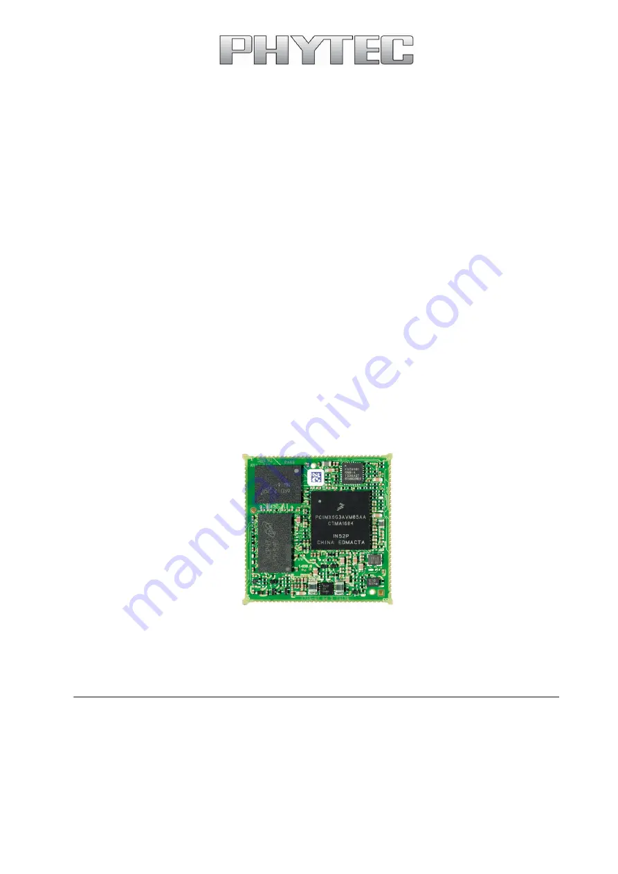
Страница 13: ...1 mm aligning all four sides of the board allowing it to be soldered like a big chip into a target application Precise specifications for the controller populating the board can be found in the appli...
Страница 14: ...available on processor type G3 Available for different temperature grades Product Temperature Grades 1 The maximum memory size listed is as of the printing of this manual Please contact PHYTEC for mor...
Страница 15: ...ORE i MX 6UL ULL Hardware Manual PHYTEC Messtecknik GmbH 15 3 2 Block Diagram FIGURE 1 Block Diagram of the phyCORE i MX 6UL ULL Note The specified direction indicated refers to the standard phyCORE u...
Страница 16: ...L 827e A3 phyCORE i MX 6UL ULL Hardware Manual PHYTEC Messtecknik GmbH 16 3 3 phyCORE i MX 6UL ULL Component Placement FIGURE 2 phyCORE i MX 6UL ULL Component Placement top view...
Страница 17: ...L 827e A3 phyCORE i MX 6UL ULL Hardware Manual PHYTEC Messtecknik GmbH 17 FIGURE 3 phyCORE i MX 6UL ULL Component Placement bottom view...
Страница 18: ...X1 90 91 92 93 Connect all 3 3 V VCC input pins to your power supply and at least the matching number of GND pins Corresponding GND X1 1 32 62 89 Please refer to Pin Description for information on add...
Страница 19: ...pads in the other corners The numbering scheme of the phyCORE i MX 6UL ULL is always in relation to the PCB as viewed from above and can be aligned with the socket of the corresponding phyCORE Carrier...
Страница 20: ...ssignment corresponding to PCB No 1468 1 for your baseboard designs For more information please refer to the product change notification LPN 228e_2 TABLE 3 Important Changes of the Pin Assignment Pin...
Страница 21: ...r the baseboard peripherals and the SOM is used e g VCC3V3 there is no need to take care of unintended current flow into the SOM since the voltages of the Peripherals and the SOM will be switched simu...
Страница 22: ...k 7 X_SD1_CMD I O VDD_3V3 uSDHC1 command 8 X_SD1_D0 I O VDD_3V3 uSDHC1 data 0 9 X_SD1_D1 I O VDD_3V3 uSDHC1 data 1 10 X_SD1_D2 I O VDD_3V3 uSDHC1 data 2 11 X_SD1_D3 I O VDD_3V3 uSDHC1 data 2 12 X_ENET...
Страница 23: ...VSYNC O VDD_3V3 LCD vertical sync 23 X_LCD_RESET O VDD_3V3 LCD reset 24 X_LCD_HSYNC O VDD_3V3 LCD horizontal sync 25 X_LCD_D0 O VDD_3V3 LCD data 0 5 26 X_LCD_D1 O VDD_3V3 LCD data 1 5 27 X_LCD_D2 O VD...
Страница 24: ...data 10 5 37 X_LCD_D11 O VDD_3V3 LCD data 11 5 38 X_LCD_D12 O VDD_3V3 LCD data 12 5 39 X_LCD_D13 O VDD_3V3 LCD data 13 5 40 X_LCD_D14 O VDD_3V3 LCD data 14 5 41 X_LCD_D15 O VDD_3V3 LCD data 15 5 42 X...
Страница 25: ...0 53 X_ENET2_TX_D1 O VDD_3V3 ETH2 RMII transmit data 1 54 X_ENET2_TX_EN O VDD_3V3 ETH2 RMII transmit enable 55 X_ENET2_TX_CLK O VDD_3V3 ETH2 RMII reference clock 56 X_ENET2_RX_D0 I VDD_3V3 ETH2 RMII...
Страница 26: ...B_OTG1_CHD_B OC i MX 6UL internal USB OTG1 charge detect 69 X_USB_OTG2_D USB_I O i MX 6UL internal USB OTG2 data 70 X_USB_OTG2_D USB_I O i MX 6UL internal USB OTG2 data 71 X_USB_OTG2_VBUS PWR_I 5 V US...
Страница 27: ...83 X_JTAG_TMS SAI2_MCLK O VDD_3V3 SAI2 7 master clock 84 X_nJTAG_TRST_B SAI2_TXD O VDD_3V3 SAI2 7 transmit data 85 X_GPIO5_3 I VDD_SNVS GPIO5_3 86 X_GPIO5_2 O VDD_SNVS GPIO5_2 CAN enable 87 X_GPIO5_1...
Страница 28: ...MX 6UL ULL ONOFF Button input 100 X_nRESET_IN I VDD_3V3 Reset input low active 101 X_SNVS_PMIC_ON_RE Q O VDD_SNVS PMIC On Request 102 X_PMIC_STBY_REQ O VDD_SNVS PMIC Standby Request 103 X_BOOT_MODE1...
Страница 29: ...4 X_FLEXCAN1_TX O VDD_3V3 FLEXCAN1 transmit 115 X_CSI_D0 I VDD_3V3 CSI data 0 116 X_CSI_D1 I VDD_3V3 CSI data 1 117 X_CSI_D2 I VDD_3V3 CSI data 2 118 X_CSI_D3 I VDD_3V3 CSI data 3 119 X_CSI_D4 I VDD_3...
Страница 30: ...round 0 V 126 GND Ground 0 V 127 GND Ground 0 V 128 GND Ground 0 V 129 GND Ground 0 V 130 GND Ground 0 V 131 GND Ground 0 V 132 GND Ground 0 V 133 GND Ground 0 V 134 GND Ground 0 V 135 GND Ground 0 V...
Страница 31: ...GND Ground 0 V 158 GND Ground 0 V 159 GND Ground 0 V 4 The specified direction indicated refers to the pins use according to the phyCORE i MX 6UL ULL specification 5 Supplies VDD_SNVS_IN and is also...
Страница 32: ...can be found in the applicable chapter listed in the table FIGURE 5 Typical Jumper Pad Numbering Scheme If manual jumper modification is required please ensure that the board as well as surrounding c...
Страница 33: ...IGURE 6 Jumper Locations top view Please pay special attention to the TYPE column to ensure you are using the correct type of jumper 0 Ohms 10k Ohms etc The jumpers are 0402 packages with a 1 8 W or b...
Страница 34: ...W bit 0 0402 EEPR OM Write Prote ction Contr ol R102 2 3 E0 0 E1 1 E2 0 0x2 0x3 W R are selected as the low nibble of the EEPROM s address I2 C memory address 0x52 ID page address 0x5A 1 2 E0 0 E1 0...
Страница 35: ...or X1 VDD_3V3 X1 90 91 92 93 Connect all 3 3 V VCC input pins to your power supply and at least the matching number of GND pins Corresponding GND X1 1 32 62 89 Please refer to Pin Description for info...
Страница 36: ...USB1 Bus voltage must be supplied with 5 V if USB1 is used X_USB_OTG2_VBUS USB2 Bus voltage must be supplied with 5 V if USB2 is used VDD_SNVS Backup supply isolated from VDD_3V3 by diode D1 Internal...
Страница 37: ...se a current flow into the controller especially if peripheral devices attached to the interfaces of the i MX 6UL ULL are supposed to be powered while the phyCORE i MX 6UL ULL is in suspend mode or tu...
Страница 38: ...tage supervisor U5 on the phyCORE module This device monitors the VDD_3V3 input voltage and reacts to other reset triggers e g of an external button too The reset delay time is typ 200 ms The reset ou...
Страница 39: ...t out at the phyCORE Connector X1 X_BOOT_MODE 1 0 pins 103 and 104 The table below shows the possible settings of pins X_BOOT_MODE0 X1 pin 104 and X_ BOOT_MODE1 X1 pin 103 and the resulting boot confi...
Страница 40: ...ormation about the eFUSEs and the impact of the settings at the BCFG pins Warning The boot mode configuration resistors must be placed on the carrier board for development Later on if the eFUSEs are u...
Страница 41: ...D_D5 I 3 3 V LCD_DATA_05 BCFG1 6 31 X_LCD_D6 I 3 3 V LCD_DATA_06 BCFG1 7 33 X_LCD_D7 I 3 3 V LCD_DATA_07 BCFG2 0 34 X_LCD_D8 I 3 3 V LCD_DATA_08 BCFG2 1 35 X_LCD_D9 I 3 3 V LCD_DATA_09 BCFG2 2 36 X_LC...
Страница 42: ...13 Options for the Boot Configuration Boot Configuration BCFG1 7 0 BCFG2 7 0 BCFG4 7 0 NAND 1Gb 64 pages p block 4 address bytes 10010010 00000000 00000000 NAND 2 4Gb 64 pages p block 5 address bytes...
Страница 43: ...L controller Refer to the i MX 6UL ULL Reference Manual for accessing and configuring these registers 9 2 NAND Flash Memory U7 Use of Flash as non volatile memory on the phyCORE i MX 6UL ULL provides...
Страница 44: ...signals E0 and E2 are fixed connected to GND The remaining chip enables signal E1 is configurable using jumper J10 The table below shows the resulting seven bit I C memory area and ID page address for...
Страница 45: ...d SD1 uSDHC1 of the i MX 6UL ULL 4 data channels Both interfaces have a maximum data rate of up to 104 MB s refer to the i MX 6UL ULL Reference Manual for more information TABLE 16 Location of the SD...
Страница 46: ...42 X_LCD_D16 I O VDD_3V3 uSDHC2 data 6 13 43 X_LCD_D17 I O VDD_3V3 uSDHC2 data 7 13 The interfaces do not provide dedicated card detect or write protect signals The card detect and write protect funct...
Страница 47: ...terface The phyCORE i MX 6UL ULL provides two high speed universal asynchronous interfaces with up to 4 MHz and one with additional hardware flow control RTS and CTS signals The following table shows...
Страница 48: ...The applicable interface signals can be found on the phyCORE Connector X1 as shown below Please note that USB2 is not available on the processor type G0 and Y0 TABLE 18 Location of the USB OTG Host S...
Страница 49: ...on board Ethernet PHY supports HP Auto MDIX technology eliminating the need for the consideration of a direct connect LAN or cross over patch cable It detects the TX and RX pins of the connected devi...
Страница 50: ...set up a second Ethernet interface on a carrier board Please note that the second Ethernet interface ENET2 is not available on the processor type Y0 G0 and G1 TABLE 20 Location of the ENET2 Interface...
Страница 51: ...select 0 112 X_ECSPI3_MISO I O VDD_3V3 ECSPI3 master input slave output 11 5 I2C Interface The Inter Integrated Circuit I2 C interface is a two wire bidirectional serial bus that provides a simple an...
Страница 52: ...hronous mode Hence the receive data timing is determined by SAI2_TX_BCLK and SAI2_TX_SYNC The five signals extending from the i MX 6UL ULL s SAI2 module to the phyCORE Connector are SAI2_RX_DATA SAI2_...
Страница 53: ...specification version 2 0B It supports standard and extended message frames and programmable bit rates of up to 1 Mb s The following table shows the position of the signals on the phyCORE Connector T...
Страница 54: ...amper detection pin 0 GPIO5_0 87 X_GPIO5_1 I O VDD_SNVS Tamper detection pin 1 GPIO5_1 85 X_GPIO5_3 I O VDD_SNVS Tamper detection pin 3 GPIO5_3 51 X_GPIO5_9 I O VDD_SNVS Tamper detection pin 9 GPIO5_9...
Страница 55: ...he desired output level A high level turns the LED on a low level turns it off FIGURE 7 User LED Location top view 14 If the phyCORE i MX 6UL ULL is equipped with the i MX 6UL ULL version G3 supportin...
Страница 56: ...3 X_JTAG_TMS SAI2_MCLK I VDD_3V3 JTAG TMS 82 X_JTAG_TDO SAI2_TX_SYNC O VDD_3V3 JTAG TDO 80 X_JTAG_TCK SAI2_RXD I VDD_3V3 JTAG clock input 84 X_JTAG_TRSTB SAI2_TXD I VDD_3V3 JTAG reset input low active...
Страница 57: ...ultiplexed in the clocking system when the system detects a loss of clock Please refer to the i MX 6UL ULL Reference Manual for more information about connecting an external clock source to the RTC TA...
Страница 58: ...Signal Location Pin Signal ST Voltage Domain Description 20 X_LCD_ENABLE O VDD_3V3 LCD enable 21 X_LCD_CLK O VDD_3V3 LCD clock 22 X_LCD_VSYNC O VDD_3V3 LCD vertical sync 23 X_LCD_RESET O VDD_3V3 LCD...
Страница 59: ...8 X_LCD_D22 O VDD_3V3 LCD data 22 49 X_LCD_D23 O VDD_3V3 LCD data 23 16 2 Supplementary Signals TABLE 30 Supplementary Signals to Support the Display Connectivity Pin Signal ST Voltage Domain Descript...
Страница 60: ...llel interfaces with 10 data bits HSYNC VSYNC MCLK and PIXCLK The upper CSI data bits D23 D10 are used for other features of the phyCORE i MX 6UL ULL FIGURE 9 Parallel Camera Interfaces at the phyCORE...
Страница 61: ...SI_D0 I VDD_3V3 CSI data 0 116 X_CSI_D1 I VDD_3V3 CSI data 1 117 X_CSI_D2 I VDD_3V3 CSI data 2 118 X_CSI_D3 I VDD_3V3 CSI data 3 119 X_CSI_D4 I VDD_3V3 CSI data 4 120 X_CSI_D5 I VDD_3V3 CSI data 5 121...
Страница 62: ...signs as reference 17 2 Utilizing the Camera Interfaces on a Carrier Board On PHYTEC carrier boards the interface is used directly as a parallel interface according to the phyCAM P standard On the tar...
Страница 63: ...wn internally In order to implement tamper protection this signal should be connected to a tamper detection contact in the application which is normally closed pulling the tamper detection signal to t...
Страница 64: ...eight of 1 2 mm microcontroller on the top side of the PCB The board itself can be easily soldered directly onto your carrier board Additional specifications TABLE 33 Technical Specifications Dimensio...
Страница 65: ...is used for active and passive parts of a SOM configuration we have categorized our SOMs into three temperature grades The table below describes these grades in detail These grades describe a set of...
Страница 66: ...Industrial 40 C to 85 C C Commercial 0 C to 95 C Consumer 0 C to 95 C Consumer 0 C to 70 C 19 2 Connectors on the phyCORE i MX 6UL ULL The phyCORE i MX 6UL ULL SOM can be directly soldered onto your c...
Страница 67: ...L Hardware Manual PHYTEC Messtecknik GmbH 67 Note To facilitate the integration of the phyCORE i MX 6UL ULL into your design the footprint of the phyCORE i MX 6UL ULL is available for download Integra...
Страница 68: ...he layout data as shown in Physical Dimensions bottom view It is available in different file formats The use of this data integrates the phyCORE i MX 6UL ULL SOM as a single component of your design d...
Страница 69: ...nges in this Manual 25 01 2017 Manual L 827e_1 First edition Describes the phyCORE i MX 6UL ULL PCB Version 1468 0 26 07 2017 Manual L 827e_2 Update to PCB Version 1468 2 Describing minor changes in p...