Circuit Descriptions, Abbreviation List, and IC Data Sheets
EN 29
LGE PDP
9.
9.2.2
Main Components
IPM, FET, DIODE, electrolytic capacitor, and E/R coil.
9.2.3
Dismantling
1.
Pull out Locks as indicated by the arrows.
2.
Condition in Lock part is pulled.
3.
Pull FPC as shown by arrow.
Figure 9-5 FPC Separating
9.3
Y Drive Board
9.3.1
Purpose
•
To supply SUSTAIN, RESET waveform which are made by
the Y SUSTAIN board and are supplied to the PDP through
the SCAN DRIVER IC.
•
To supply a waveform that selects the horizontal electrode
(Y SUSTAIN electrode) sequentially.
–
Potential difference is 0 V between GND and Vpp of
DRIVER IC in SUSTAIN period.
–
Being generated potential difference between GND
and Vpp only in SCAN period.
Note: In case of 42” V7, used DRIVER SCAN ICs are in total
of 8 EA (TOP, BOTTOM: each 4 EA).
Figure 9-6 Y Drive board
9.4
Y Sustain Board
9.4.1
Purpose
Generates SUSTAIN, RESET, and Vsc (SCAN) voltages, and
supplies them to the Y DRIVE board.
Figure 9-7 Y Sustain board
9.4.2
Main Components
IPM, diode, electrolytic capacitor, and FET.
9.5
Control Board
9.5.1
Purpose
Creates signal processing, and controls many FET on each
DRIVER board with R, G, and B signals.
Firstly receive 5 V, and then use two voltages (3.3 V / 1.8 V).
Figure 9-8 Control board
F_15590_052.eps
040705
•Y DRIVER
SCAN IC
Status Separated
with Y-SUS B/D
Status Assembled
F_15590_053.eps
040705
F_15590_054.eps
040705
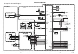
* IPM (Intelligent Power Module)
E/R(Energy recovery)
MCM
( Multi Chip Module)
LVDS Signal
Input pin
MCM
( Multi Chip Module )
6 bi t
signal
8 bit or 10
bit signal
TCP
F_15590_055.eps
040705


