


1
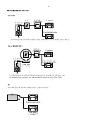
PLAYABILITY CHECK
For sets which are compatible with
CD-RW
discs
use CD-RW Printed Audio Disc ....................7104 099 96611
TR 3 (Fingerprint)
TR 8 (600µ Black dot)
maximum at 01:00
• playback of these two tracks without audible disturbance
playing time for: Fingerprint 10seconds
Black dot from 00:50 to 01:10
• jump forward/backward (search) within a reasonable time
For all other sets
use CD-DA SBC 444A..................................4822 397 30245
TR 14 (600µ Black dot)
maximum at 01:15
TR 19 (Fingerprint)
TR 10 (1000µ wedge)
• playback of all these tracks without audible disturbance
playing time for: 1000µ wedge 10seconds
Fingerprint 10seconds
Black dot from 01:05 to 01:25
• jump forward/backward (search) within a reasonable time
2
CUSTOMER INFORMATION
It is proposed to add an addendum sheet to the set which
informs the customer that the set has been checked
carefully - but no fault was found.
The problem was obviously caused by a scratched, dirty or
copy-protected CD. In case problems remain, the customer
is requested to contact the workshop directly.
The lens cleaning (method
3
) should be mentioned in the
addendum sheet.
The final wording in national language as well as the printing
is under responsibility of the Regional Service Organizations.
4
LIQUID LENS CLEANING
Because the material of the lens is synthetic and coated
with a special anti-reflectivity layer, cleaning must be done
with a non-aggressive cleaning fluid. It is advised to use
“Cleaning Solvent
The actuator is a very precise mechanical component and
may not be damaged in order to guarantee its full function.
Clean the lens gently (don’t press too hard) with a soft and
clean cotton bud moistened with the special lens cleaner.
The direction of cleaning must be in the way as indicated in
the picture below.
Before touching the lens it is advised to clean the
surface of the lens by blowing clean air over it.
This to avoid that little particles make scratches on
the lens.
INSTRUCTIONS ON CD PLAYABILITY
1 - 7
Содержание MCD355
Страница 2: ...1 2 PCBS LOCATION ...
Страница 8: ...3 1 3 1 SET BLOCK DIAGRAM ...
Страница 9: ...SET WIRING DIAGRAM 4 1 4 1 ...
Страница 11: ...5 2 5 2 PCB LAYOUT MAIN BOARD TOP VIEW ...
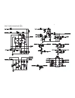
Страница 12: ...5 3 5 3 CIRCUIT DIAGRAM MAIN BOARD PART1 ...
Страница 13: ...5 4 5 4 CIRCUIT DIAGRAM MAIN BOARD PART2 ...
Страница 14: ...5 5 5 5 CIRCUIT DIAGRAM MAIN BOARD PART3 ...
Страница 15: ...5 6 5 6 CIRCUIT DIAGRAM MAIN BOARD PART4 ...
Страница 16: ...5 7 5 7 CIRCUIT DIAGRAM MAIN BOARD PART5 ...
Страница 17: ...5 8 5 8 CIRCUIT DIAGRAM MAIN BOARD PART6 ...
Страница 18: ...5 9 5 9 CIRCUIT DIAGRAM MAIN BOARD PART7 ...
Страница 19: ...5 10 5 10 CIRCUIT DIAGRAM MAIN BOARD PART8 ...
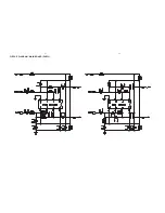
Страница 20: ...5 11 5 11 PCB LAYOUT HEADPHONE JACK BOARD CIRCUIT DIAGRAM HEADPHONE JACK BOARD ...
Страница 21: ...5 12 5 12 PCB LAYOUT AUX JACK BOARD CIRCUIT DIAGRAM AUX JACK BOARD ...
Страница 23: ...6 2 6 2 PCB LAYOUT VFD BOARD TOP VIEW ...
Страница 24: ...PCB LAYOUT DISPLAY PANEL BOARD BOTTOM VIEW 6 3 6 3 ...
Страница 25: ...6 4 6 4 CIRCUIT DIAGRAM VFD BOARD PART1 ...
Страница 26: ...6 5 6 5 CIRCUIT DIAGRAM VFD BOARD PART2 ...
Страница 27: ...6 6 6 6 CIRCUIT DIAGRAM VFD BOARD PART3 ...
Страница 28: ...6 7 6 7 PCB LAYOUT TOUCH KEY BOARD ...
Страница 29: ...6 8 6 8 CIRCUIT DIAGRAM TOUCH KEY BOARD ...
Страница 31: ...7 2 7 2 PCB LAYOUT SERVO BOARD TOP VIEW ...
Страница 32: ...7 3 7 3 PCB LAYOUT SERVO BOARD BOTTOM VIEW ...
Страница 33: ...7 4 7 4 CIRCUIT DIAGRAM SERVO BOARD PART1 ...
Страница 34: ...7 5 7 5 CIRCUIT DIAGRAM SERVO BOARD PART2 ...
Страница 35: ...7 6 7 6 CIRCUIT DIAGRAM SERVO BOARD PART3 ...
Страница 36: ...7 7 7 7 CIRCUIT DIAGRAM SERVO BOARD PART4 ...
Страница 37: ...7 8 7 8 CIRCUIT DIAGRAM SERVO BOARD PART5 ...
Страница 38: ...7 9 7 9 CIRCUIT DIAGRAM SERVO BOARD PART6 ...
Страница 39: ...7 10 7 10 CIRCUIT DIAGRAM SERVO BOARD PART7 ...
Страница 40: ...7 11 7 11 CIRCUIT DIAGRAM SERVO BOARD PART8 ...
Страница 41: ...7 12 7 12 CIRCUIT DIAGRAM SERVO BOARD PART9 ...
Страница 42: ...USB POWER KEY BOARD 8 1 8 1 ...
Страница 43: ...8 2 8 2 PCB LAYOUT USB JACK BOARD CIRCUIT DIAGRAM USB JACK BOARD ...
Страница 44: ...PCB LAYOUT POWER KEY BOARD 8 3 8 3 CIRCUIT DIAGRAM POWER KEY BOARD ...
Страница 45: ...3 7 B 6 D A G 4 2 14 13 C 5 10 11 8 1 9 8 1 8 1 SET MECHANICAL EXPLODED VIEW ...