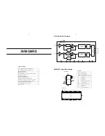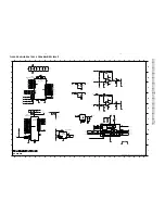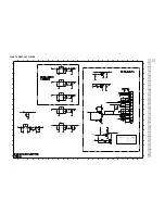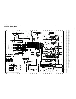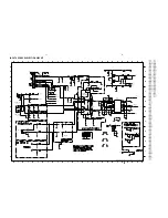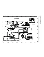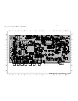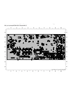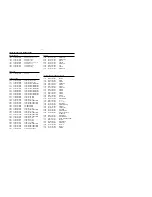
AMPLIFIER BOARD
TABLE OF CONTENTS
Class-D Amplifier circuit description ................................................. 8-1
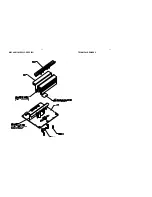
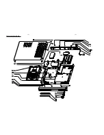
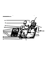
Exploded view ................................................................................... 8-2
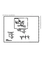
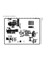
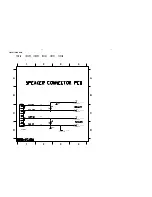
Class-D Amplifier Board- Circuit Diagram Part 1 .............................. 8-3
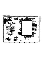
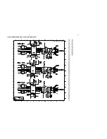
Class-D Amplifier Board- Circuit Diagram Part 2 .............................. 8-4
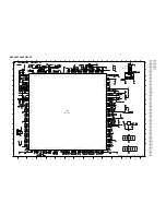
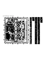
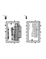
Class-D Amplifier Board- Top View Layout ....................................... 8-5
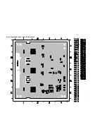
Class-D Amplifier Board- Bottom View Layout ................................. 8-6
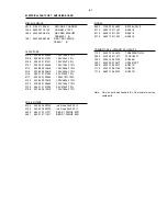
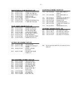
Electrical parts list - Amplifier board ................................................. 8-7
8-1
8-1
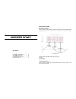
6-channel class-D amplifier
Basic operation of a class-D amplifier
Basically, the output stage of a class-D amplifier outputs a continuous square wave swinging between positive and negative power supplies
with a fixed frequency (“clock” frequency) far beyond the audible range. The duty cycle of this square wave is modulated with the audio signal.
The output is followed by a low-pass filter which eliminates the clock frequency and allows only the audio signal going to the speaker. See
simplified drawing below.
Compared to a conventional power amplifier the benefits of the Class-D amplifier are:
• higher effiency
• lower power dissipation
• smaller heatsink required
• smaller mains transformer required
The main disadvantage of this concept is:
• The amplifier is operating with a high-frequency square wave at high amplitude and currents. This requires special precautions to prevent
excessive electromagnetic ratiation (EMC).
Содержание LX2600D
Страница 11: ...4 1 4 1 SET BLOCK DIAGRAM TUNER TM 08 TDA8922 L R POWER AMP Lx2600D 97 Block Diagram_39331_HY_wk443 2 ...
Страница 32: ...7 10 7 10 PCB 3139 113 3522 pt3 TOP VIEW Use by LX2600D 97 LX2600D_AV Mono_31391133522 pt 3_HY_wk433 2 ...
Страница 33: ...7 11 7 11 PCB 31311352 pt3 TOP VIEW MAPPING ...
Страница 34: ...7 12 7 12 PCB 3139 113 3522 pt3 BOTTOM VIEW Use by LX2600D 97 LX2600D_3139 113 3522 pt3_HYwk0442 ...
Страница 35: ...7 13 7 13 PCB 3139 113 3522 pt3 BOTTOM VIEW MAPPING ...
Страница 38: ...8 2 8 2 MECHANICAL EXPLODED VIEW 0010 0006 TECHNICAL REMARKS ...
Страница 46: ...9 3 9 3 COMPONENT LAYOUT CHIP LAYOUT 3139_113_3595 1 circuit1 _HY_wk0442 3139_113_3595 1 circuit1 _HY_wk0442 ...
Страница 47: ...MAIN ENCASING EXPLODED VIEW 10 1 10 1 ...
Страница 48: ...MAIN ENCASING EXPLODED VIEW 10 2 10 2 ...

