background image

Service Modes, Error Codes, and Fault Finding

EN 17

LC4.41A AA

5.

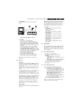
How to Connect

This is described in the chassis fault finding database in 
ComPair. 

Figure 5-6 ComPair interface connection

How to Order

ComPair order codes (EU/AP/LATAM):

Starter kit ComPair32/SearchMan32 software and 
ComPair interface (excl. transformer): 3122 785 90450.

ComPair interface (excl. transformer): 4822 727 21631.

Starter kit ComPair32 software (registration version): 3122 
785 60040.

Starter kit SearchMan32 software: 3122 785 60050.

ComPair32 CD (update): 3122 785 60070 (year 2002), 
3122 785 60110 (year 2003 onwards).

SearchMan32 CD (update): 3122 785 60080 (year 2002), 
3122 785 60120 (year 2003), 3122 785 60130 (year 2004).

ComPair firmware upgrade IC: 3122 785 90510.

Transformer (non-UK): 4822 727 21632.

Transformer (UK): 4822 727 21633.

ComPair interface cable: 3122 785 90004.

ComPair interface extension cable: 3139 131 03791.

ComPair UART interface cable: 3122 785 90630.

Note:

 If you encounter any problems, contact your local 

support desk.

5.4.2

LVDS Tool

Introduction

This service tool (also called “ComPair Assistant 1“) may help 
you to identify, in case the TV does not show any picture, 
whether the Small Signal Board (SSB) 

or 

the display of a Flat 

TV is defective. 
Furthermore it is possible to program EPLDs with this tool (Byte 
blaster). Read the user manual for an explanation of this 
feature.

Since 2004, the LVDS output connectors in our Flat TV models 
are standardised (with some exceptions). With the two 
delivered LVDS interface cables (31p and 20p) you can cover 
most chassis (in special cases, an extra cable will be offered).

When operating, the tool will show a small (scaled) picture on 
a VGA monitor. Due to a limited memory capacity, it is not 
possible to increase the size when processing high-resolution 
LVDS signals (> 1280x960). Below this resolution, or when a 
DVI monitor is used, the displayed picture will be full size. 

Generally this tool is intended to determine if the SSB is 
working or not. Thus to determine if LVDS, RGB, and sync 
signals are okay.

How to Connect

Connections are explained in the user manual, which is packed 
with the tool. 

Note:

 To use the LVDS tool, you must have ComPair release 

2004-1 (or later) on your PC (engine version >= 2.2.05). 
For every TV type number and screen size, one must choose 
the proper settings via ComPair. The ComPair file will be 
updated regularly with new introduced chassis information. 

How to Order

LVDS tool (incl. two LVDS cables: 31p and 20p): 
3122 785 90671.

LVDS tool Service Manual: 
3122 785 00810.

LVDS cable 31p/FI -> 31p/FI (for JL2.1 chassis):
3122 785 90861.

LVDS cable 30p/DF -> 31p/FI (for LC4.3 chassis): 
3122 785 90821.

LVDS cable 41p/FI -> 31p/FI (dual -> single LVDS): 
3122 785 90831.

LVDS cable 20p/DF -> 20p/DF (standard with tool):
3122 785 90731.

LVDS cable 31p/FI -> 31p/FI (standard with tool):
3122 785 90662.

LVDS cable 20p/DF -> 20p/DF (for LC4.1 chassis):
3122 785 90851.

5.5

Error Codes

The error code buffer contains all errors detected since the last 
time the buffer was erased. The buffer is written from left to 
right. When an error occurs that is not yet in the error code 
buffer, it is displayed at the left side and all other errors shift one 
position to the right.

5.5.1

How to Read the Error Buffer

You can read the error buffer in 3 ways:

On screen via the SAM (if you have a picture). 

Examples:

ERROR: 0 0 0 0 0 : No errors detected

ERROR: 6 0 0 0 0 : Error code 6 is the last and only 
detected error

ERROR: 9 6 0 0 0 : Error code 6 was detected first and 
error code 9 is the last detected (newest) error

Via the blinking LED procedure (when you have no 
picture). See “The Blinking LED Procedure”.

Via  ComPair.

5.5.2

How to Clear the Error Buffer

The error code buffer is cleared in the following cases:

By using the CLEAR command in the SAM menu:

To enter SAM, press the following key sequence on the 
remote control transmitter: “

062596

” directly followed 

by the OSD/i+ button (do not allow the display to time 
out between entries while keying the sequence).

Make sure the menu item CLEAR is selected. Use the 
MENU UP/DOWN buttons, if necessary.

Press the MENU RIGHT button to clear the error 
buffer. The text on the right side of the “CLEAR” line will 
change from “CLEAR?” to “CLEARED”

If the contents of the error buffer have not changed for 50 
hours, the error buffer resets automatically.


Note: 

If you exit SAM by disconnecting the mains from the 

television set, the error buffer is not reset.

E_06532_021.eps

180804

PC

VCR

I2C

Power
9V DC

 TO

UART SERVICE

CONNECTOR

 TO

I2C SERVICE

CONNECTOR

Содержание LC4.41A AA

Страница 1: ...am Audio Control 23 Test Point Overview Small Signal Board 24 I2C Overview 25 Supply Voltage Overview 26 7 Circuit Diagrams and PWB Layouts Diagram PWB SSB Tuner and IF B1 27 49 58 SSB Hercules B2 28 49 58 SSB Sync Interface B3 29 49 58 SSB Audio Delay Line PDP Only B4 30 49 58 SSB Audio Processing B5 31 49 58 SSB DC DC Converter B6 32 49 58 SSB Diversity Tables B1 B6 33 SSB Scaler B7 34 49 58 SSB...

Страница 2: ... G D K I SECAM B G D K L L Video playback NTSC M N 3 58 4 43 PAL B G SECAM L L Supported computer formats VGA 640x480 MAC 640x480 SVGA 800x600 XVGA 1024x768 Supported video formats 640x480p 2fH 720x576p 2fH 1280x720p 3fH 1920x1080i 2fH Presets channels 100 presets Tuner bands VHF UHF S band Hyper band 1 1 2 Sound Sound systems NICAM B G D K I L AV Stereo Maximum power WRMS 2 x 15 1 1 3 Miscellaneo...

Страница 3: ...19 HPD Hot Plug Detect j 20 Ground Gnd H Cinch DVI Audio In Rd Audio R 0 5 VRMS 10 kohm jq Wh Audio L 0 5 VRMS 10 kohm jq CVI 2 VGA Video RGB In Figure 1 3 VGA Connector 1 Video Red 0 7 VPP 75 ohm j 2 Video Green 0 7 VPP 75 ohm j 3 Video Blue 0 7 VPP 75 ohm j 4 n c 5 Ground Gnd H 6 Ground Red Gnd H 7 Ground Green Gnd H 8 Ground Blue Gnd H 9 5VDC 5 V j 10 Ground Sync Gnd H 11 n c 12 DDC_SDA DDC dat...

Страница 4: ...ations Connections and Chassis Overview EN 4 LC4 41A AA 1 1 3 Chassis Overview Figure 1 4 PWB CBA locations G_16160_036 eps 260706 B SMALL SIGNAL BOARD D SIDE I O PANEL J LED PANEL E CONTROL PANEL C AUDIO AMPLIFIER PANEL ...

Страница 5: ...3 kHz R 1 kHz unless stated otherwise and picture carrier at 475 25 MHz for PAL or 61 25 MHz for NTSC channel 3 Where necessary measure the waveforms and voltages with D and without E aerial signal Measure the voltages in the power supply section both in normal operation G and in stand by F These values are indicated by means of the appropriate symbols The semiconductors indicated in the circuit d...

Страница 6: ...high steam pressure inside the body If the packaging was opened before usage the IC has to be heated up for some hours around 90 C for drying think of ESD protection Do not re use BGAs at all For sets produced before 1 1 2005 containing leaded soldering tin and components all needed spare parts will be available till the end of the service period For the repair of such sets nothing changes In case...

Страница 7: ...Directions for Use EN 7 LC4 41A AA 3 3 Directions for Use You can download this information from the following websites http www philips com support http www p4c philips com ...

Страница 8: ... dressing 4 2 Service Position 4 3 Assy Panel Removal 4 4 Set Re assembly Notes Figures below can deviate slightly from the actual situation due to the different set executions Follow the disassembling instructions in described order 4 1 Cable dressing Figure 4 1 Cable dressing G_16160_037 eps 200706 ...

Страница 9: ...Make sure that wires and other internal components are not damaged during cover removal 4 3 2 Side I O Panel Figure 4 3 Side I O panel 1 Remove the rear panel 2 Remove the screw from the cable clip 1 3 Remove the screws 2 from the loudspeaker cabinet 4 Lift the loudspeaker cabinet from the frame 5 Disconnect the cable 3 from the panel 6 Remove the fixation screws 4 and slide the panel out of its b...

Страница 10: ...e a few centimetres away from the connector plate see Figure SSB shield 6 Remove the fixation screws 5 and lift the shield from the SSB module 7 Disconnect connector 6 see Figure SSB panel 8 Unlock the catches 7 and lift the OTC TXT panel from the SSB panel 9 Remove the fixation screws 8 10 Remove the SSB panel Figure 4 8 SSB shield Figure 4 9 SSB panel 4 3 6 Audio Amplifier Panel Figure 4 10 Audi...

Страница 11: ...hanical Instructions EN 11 LC4 41A AA 4 4 3 7 Plasma Panel Figure 4 11 Plasma panel removal 1 3 Figure 4 12 Plasma panel removal 2 3 G_16240_020 eps 160206 2 1 3 4 G_16240_021 eps 170206 8 9 7 6 5 9 10 10 ...

Страница 12: ...mp 10 Release all disconnected cables from the mostly plastic guidances on the frame 11 Loosen screws 9 12 Lift the metal frame 10 together with the SSB from the plasma panel 13 Cautiously unplug the LVDS connector 11 from the Logic Board of the Plasma panel see Figure Logic Board Be careful as this is a very fragile connector cable 14 Remove the bronze spacer 12 from the stud on the plasma panel ...

Страница 13: ... error buffer To check the life timer Specifications Table 5 1 SDM default settings All picture settings at 50 brightness colour contrast hue Bass treble and balance at 50 volume at 25 All service unfriendly modes if present are disabled The service unfriendly modes are Timer Sleep timer Child parental lock Blue mute Hotel hospital mode Auto shut off when no IDENT video signal is received for 15 m...

Страница 14: ...hours but does not count standby hours 2 AAAAABC X YY This is the software identification of the main microprocessor A the project name B the region E Europe A Asia Pacific U NAFTA L LATAM C the language cluster number X the main software version number updated with a major change that is incompatible with previous versions Y the sub software version number updated with a minor change that is comp...

Страница 15: ...call centre to diagnose problems and failures in the TV set before making a service call The CSM is a read only mode therefore modifications are not possible in this mode How to Enter To enter CSM press the following key sequence on the remote control transmitter 123654 do not allow the display to time out between entries while keying the sequence Upon entering the Customer Service Mode the follow...

Страница 16: ... to select STORE 8 Press the MENU RIGHT key to store the new value 9 Press the MENU key to exit the PERSONAL picture mode 5 4 Service Tools 5 4 1 ComPair Introduction ComPair Computer Aided Repair is a service tool for Philips Consumer Electronics products ComPair is a further development on the European DST service remote control which allows faster and more accurate diagnostics ComPair has three...

Страница 17: ...you must have ComPair release 2004 1 or later on your PC engine version 2 2 05 For every TV type number and screen size one must choose the proper settings via ComPair The ComPair file will be updated regularly with new introduced chassis information How to Order LVDS tool incl two LVDS cables 31p and 20p 3122 785 90671 LVDS tool Service Manual 3122 785 00810 LVDS cable 31p FI 31p FI for JL2 1 cha...

Страница 18: ...ne with the NVM Editor in SAM mode With this option single bytes can be changed Caution Do not change the NVM settings without understanding the function of each setting because incorrect NVM settings may seriously hamper the correct functioning of the TV set Do not change the Scaler NVM settings as this will hamper the DVI HDMI functionality of the TV set Always note down the existing NVM setting...

Страница 19: ...ling horizontal lines for EU sets only 1 Check whether AGC L in SAM mode is set to 0 2 If yes align the set to correct value Required System is not Selected Correctly Check whether a Service jumper 4204 4205 0805 size is present If yes remove it 5 7 5 Video Processing No Power 1 Check 12 V and 3V3 at position 1J02 2 If no supply first check the connector 1J02 3 If the connector is correct check th...

Страница 20: ...Service Modes Error Codes and Fault Finding EN 20 LC4 41A AA 5 Personal Notes E_06532_012 eps 131004 ...

Страница 21: ...P Y MAIN DRIVING BOARD D SIDE I O E CONTROL BOARD J LED PANEL PLASMA PANEL FILTER AC Supply 8187 RIGHT SPEAKER LEFT SPEAKER 8P9 CN4004 8P11 G_16160_032 eps 250706 CN1M10 4P 8900 WIRING 42 50 SDI CN1M03 10P CN1M46 11P Shielding 8321 TUNER B SSB 1J04 9P 1N17 31P 1J03 3P 1K02 3P 1K04 11P 1K00 6P 1J01 11P 1442 14P 1J00 10P LVDS 31P 8P06 8136 8870 8101 C AUDIO 1M03 2P3 1M04 2P3 1M01 9P 1M02 7P 8903 890...

Страница 22: ...2 EF 7L71 7L01 P3563M LF A D CONV COL_Di 1 9 COL_YA 1 9 COL_A COL_DQ 7M00 T6TU5XBG COLUMBUS DIGITAL COMB FILTER DRAM 512Kx16x2 7M01 MSM56V16 2V5_DDR 95 G_16160_024 eps 190706 9 6 11 2 3 37 38 SCL SDA COL_Do 1 8 COL_YB 1 8 7E00 1 13 3 5 2 12 15 14 4 C3 SOG 2 1304 1M36 1K01 1K04 2 4 4 1 5 SVHS 2 4 3 1301 1001 1302 1002 64 58 FRONT_Y_CVBS_IN FRONT_C_IN 59 SC2_AV3_C_IN CVI_Pr_IN CVI_Y_IN CVI_Pb_IN SC1...

Страница 23: ...SEMISTANDBY 1703 Menu 1M01 2 2 1K02 KEYBOARD 3V3STBY P50_LIN2_ITV_IR_SW_RST 123 1202 24M576 7601 TS482ID 1 7 2 6 11 10 1010 7 1 2 11 11 DETECT HP_DET_R_DC_1 HP_DET_R_DC_1 EXT_MUTE 2 1 9 10 7602 74HC08PW B16 B2 B2 6 8 OUT_MUTE 3 5 3432 RES 7756 3759 3750 3V3STBY 3V3SW SC_STANDBY 7755 PANEL PWR CTL 3758 3755 LVDS_VCC 5756 5757 PAN_VCC 12VSW B8 CVI 1 AUDIO L R IN 7758 7754 2 HD_AudioINL HD_AudioINR H...

Страница 24: ...212 B3 I213 B3 I214 C3 I215 B3 I217 C4 I218 B4 I219 B4 I220 C4 I221 B2 I222 B3 I223 B2 I224 B4 I225 B3 I226 C3 I227 C3 I228 B4 I229 C3 I230 B4 I231 C3 I232 B2 I233 C3 I234 C2 I235 B2 I236 B2 I237 C2 I238 B2 I239 B4 I240 B4 I241 A3 I242 A3 I243 B4 I244 C4 I246 B4 I247 B4 I248 B4 I254 D4 I255 B4 I256 B4 I257 B4 I258 C3 I259 C4 I262 B2 I264 B2 I265 C4 I266 C4 I267 C4 I268 B4 I269 B2 I270 C4 I271 B4 I...

Страница 25: ...UART UART_TX UART_RX 3122 3123 M1 M2 2 1802 1 JTAG_TDI_SDA JTAG_CLK_SCL AF7 AD6 3V3_IO 3838 3837 JTAG I2C FSDATA FSADDR OCMDATA OCMADDR 7 SWHW_I2C_SDA SWHW_I2C_SCL 1 1G03 2 Reserved for DMMI 38 37 7L01 P3563M ADC ERR 7 3L19 3L18 A15 B15 7M00 T6TU5XBG COLUMBUS CTRL ERR 11 3M14 3M15 ERR 17 198 200 7N00 T6TF4AFG PACIFIC3 MISC ERR 16 1N04 2 3 4 FOR DEVELOPMENT USE ONLY N S SDA SCL 1 3V3SW 3N20 3N21 7A...

Страница 26: ...V_UFD 5J03 1J07 1J08 N C N C N C N C 4J01 5V 1 1J00 1M03 2 3 4 5 6 7 8 9 10 STANDBY FAN_SPEED BACKLIGHT_CTRL N C LAMP_ON_OFF POWER_UP_OK N C N C PROTECT_AUD UFD CONTROL B3 B6 B5 B6 B9 B6 B6 B16 B16 B6 B6 B6 B6 B16 B6 B6 B8 B4 B9 B19 B19 B6 B6 B20 B6 B6 12VSW 3V3STBY 7708 IN OUT COM 5V 5V 5704 8VSW_TV 7738 IN OUT COM 5738 7754 LVDS_VCC 7758 3V3SW PANEL PWR CTL 5752 DC DC Converter 7752 5753 5754 5V...

Страница 27: ...F3 I101 C2 I102 B6 I103 C5 I104 D5 I105 D5 I106 D6 I110 D7 I112 C1 I113 C1 NC1 6 NC2 10 4 SCL 5 SDA TU 2 ADC AGC 1 AS 3 IFOUT 11 12 13 14 15 16 17 TUNER UV1318ST AIH MK3 1102 33V 9 5V 7 8 3101 100R 100R 3102 4115 4116 2114 1u0 100u 2113 I113 16V I112 3127 100R 100R 3126 100R 3125 3124 100R 5VSW_b 5VSW_a VTUN 5VSW_a 5VSW_a 5VSW_b 10n 2102 2101 100u 16V 3106 14 15 2 3 11 12 16 17 7 8 1 18 4 5 6 9 10...

Страница 28: ...244 B7 I246 D2 I247 D4 I248 D4 I254 F6 I255 F6 I256 E7 I257 E7 I258 E7 I259 F8 I262 F8 I264 F9 I265 F10 I266 F10 I267 F11 I268 G11 I269 C11 I270 B11 I271 B10 I272 B10 I273 C9 I274 A9 I275 A9 I277 C8 I278 C8 I283 B6 I284 B6 I285 B6 I288 B6 I289 A3 I290 A3 I291 A4 I292 B3 I293 B3 I294 B3 I297 B8 I298 C7 B3 SFSKA 1201 2 1 3 F252 F251 6 3V 330u 2204 3V3STBY 6 3V 330u 2222 4K7 3299 F217 3221 3261 F263 ...

Страница 29: ... A8 I453 B3 I454 B2 I455 E2 5V I455 F406 F404 F405 F408 F407 F409 F411 F410 F412 3V3SW 2 3 4 5 6 7 8 9 15 16 BM14B SRSS TB 1442 1 10 11 12 13 14 I454 I453 3463 3V3SW 2449 100n 3V3SW 100R 3462 4439 3461 100R 4441 3459 3V3SW 100R 100R 3V3SW 3458 4440 3456 100R 100R 3455 100R 3454 12 3453 100R 7436 6 74LVC14APW 13 7 14 11 7 14 10 9 7 14 8 7436 5 74LVC14APW 14 6 7436 4 74LVC14APW 7436 3 74LVC14APW 5 7...

Страница 30: ...07 C9 4508 C9 4509 C9 4510 C9 4511 C9 4512 C9 4513 C9 4514 C9 5501 A1 7501 A1 7502 B3 7503 F1 7504 F6 7505 B7 7506 B8 F501 A2 F502 B2 F503 C10 F504 D10 F505 F10 I501 F5 I502 F6 I503 E2 I504 E2 I506 I507 I504 I503 22 28 27 F502 5 20 11 12 13 15 16 17 18 19 14 8 9 10 24 25 26 1 2 3 4 RAM 32kx8 7502 CY62256LL 70ZC 21 23 6 7 2508 82p 2507 470p 20 2506 330p 11 1 19 18 17 16 15 14 13 12 2 3 4 5 6 7 8 9 ...

Страница 31: ...I608 A5 I610 B5 I611 C7 I612 D7 I613 E3 I614 E4 I615 E4 I616 E8 I617 F5 I618 A6 I619 D8 I620 D2 I621 D7 I620 I621 2619 4606 6 3V 47u 4621 5V 4620 4619 3V3STBY 4618 4617 4616 4614 4613 4615 4612 4611 4610 39R 3633 4609 3632 39R 3628 5V 3629 3631 470R 3630 470R 5VSW 10K 3627 22K 3626 I619 I618 I616 6601 BZX384 C3V3 I617 I615 I613 I614 I611 I612 I610 4603 I608 3625 3K3 4601 5VSW 100n 2614 5VSW BC847B...

Страница 32: ... F6 2737 H6 2738 G1 2739 G2 2741 H2 2749 B8 2750 F9 2751 B9 2752 B10 2759 100u 16V 10K 3702 10K 3701 SIG_GND2 I764 100n 2702 I762 I704 4 3 I701 I702 SI4922DY 7711 2 5 6 15K 3724 SIG_GND2 SUP_GND2 SUP_GND2 SIG_GND2 SIG_GND2 SIG_GND2 I724 I726 F717 I720 I721 I718 I719 I716 I714 I715 10R 3718 I717 I712 I711 I722 I723 SS24 6718 I725 1 1K0 5717 10u 3727 10R 3723 1 1n0 2725 470u 3725 3K3 1K2 2726 16V 37...

Страница 33: ...2190030 RST SM 0603 JUMP 0R05 COL 4602 319802190030 RST SM 0603 JUMP 0R05 COL 4603 319802190030 RST SM 0603 JUMP 0R05 COL 4606 319802190030 RST SM 0603 JUMP 0R05 COL 4609 319802190030 RST SM 0603 JUMP 0R05 COL 4610 319802190030 RST SM 0603 JUMP 0R05 COL 4611 319802190030 RST SM 0603 JUMP 0R05 COL 4612 319802190030 RST SM 0603 JUMP 0R05 COL 4613 319802190030 RST SM 0603 JUMP 0R05 COL 4614 319802190...

Страница 34: ...B0 JTAG_CLK DORED0 AE6 GPIO_G08_B1 JTAG_MODE DORED1 AF6 GPIO_G08_B2 JTAG_TDI DOGRN0 AE7 GPIO_G08_B3 DVS DOGRN1 AF7 GPIO_G08_B4 JTAG_TDO DOBLU0 AD8 GPIO_G08_B5 JTAG_RESET DOBLU1 AE4 GPIO_G09_B0 DERED0 AF18 GPIO_G06_B3 DORED5 GPIO_G07_B0 DERED2 AE8 AF8 GPIO_G07_B1 DERED3 AC9 GPIO_G07_B2 DERED4 AD9 GPIO_G07_B3 DERED5 AE9 GPIO_G07_B4 DERED6 AF9 GPIO_G07_B5 DERED7 AD10 GPIO_G07_B6 DERED8 AF26 GPIO_G04_...

Страница 35: ... A9 RX1p B10 RX2n RX2p A10 B6 RXCn A6 RXCp 1V8_DVI B7 C7 D7 D11 N4 DVI_SCL GPI_07 N3 DVI_SDA GPI_08 B11 REXT B8 RX0n A8 D9 D10 C6 C8 C9 C10 C11 A7 A11 B5 7801 2 DVI D6 D8 4900 2942 100n C12 LBADC_IN1 B12 LBADC_IN2 A12 LBADC_IN3 D12 LBADC_RETURN 3V3_LBADC 7801 3 ADC C13 D13 A1 C5 D5 AC17 K3 F1 VSSD33_LVDS AD17 7801 14 NC LVDSA_GND_3 AC20 LVDSB_3 3_1 AD12 LVDSB_3 3_2 AD13 LVDSB_3 3_3 AC12 LVDSB_GND_...

Страница 36: ... BCp DEGRN8 AE12 SHIELD0 DEGRN2 AF10 SHIELD1 DEGRN3 AC11 SHIELD2 DEGRN4 AD11 SHIELD3 DEGRN5 AE11 SHIELD4 DEBLU2 AE13 AE20 B0n DEBLU9 AE16 B0p DEBLU8 AF16 B1n DEBLU7 AE15 B1p DEBLU6 AF15 B2n DEBLU4 AE14 B2p DEBLU3 AF14 B3n DEGRN7 AF12 AE23 A1n GPIO_G05_B5 DOGRN7 AF22 A1p GPIO_G05_B4 DOGRN6 AE22 A2n GPIO_G05_B2 DOGRN4 AF21 A2p GPIO_G05_B1 DOGRN3 AE21 A3n GPIO_G06_B5 DORED7 AF19 A3p GPIO_G06_B4 DORED...

Страница 37: ...7 93 15 35 7 60 61 94 52 38 89 90 91 39 40 77 78 80 81 1 83 84 3 4 6 10 12 13 100 17 18 20 21 74 75 24 57 97 98 63 64 68 69 71 72 9 45 29 30 26 55 53 54 28 23 56 32 36 37 33 34 47 48 49 50 51 Φ SDRAM 1M X 32 X 4 K4D263238F UC50 7B01 31 100n 2B16 2V5_DDR 100n 2B15 2B14 100n 100n 2B13 2B12 100n 100n 2B11 2B10 100n 100n 2B09 2B08 100n 100n 2B07 2B06 100n 100n 2B05 2B04 100n 100n 2B03 6 3V 47u 2B02 2B...

Страница 38: ...400DT 55N6 25 24 6 3C17 10K 1 3 2 4 1C00 SKQR 3V3_IO 3C05 10K 10K 3C04 4 4 5 10K 3 6 10K 3C04 2 2 7 3C04 3 1 8 3C04 1 10K FC06 FC10 FC07 FC09 FC08 FC04 FC05 FC02 FC03 FC00 FC01 4 5 3V3SW 3 6 3C06 4 10K 2 7 3C06 3 10K 8 3C06 2 10K 3C06 1 10K 1 10K 3C07 4 4 5 10K 3C07 3 3 6 10K 3C07 2 2 7 1 8 4 5 10K 3C07 1 6 3C08 4 10K 3C08 3 10K 3 3C08 2 10K 2 7 3C08 1 10K 1 8 2C00 10K 100n 3C18 3C21 3C20 4 5 3V3_...

Страница 39: ...PLL 22u 6 3V 2D02 5D06 FD12 2D09 1n0 1n0 VDDA_3V3 2D08 1n0 2D12 3D02 4K7 4K7 3D00 VDDD_1V8 1 3D08 1K0 1 1K0 3D07 ID10 2D49 2D38 1n0 1n0 1n0 2D39 2D37 1n0 2D36 1n0 1n0 2D35 2D34 1n0 1n0 2D32 1n0 2D30 2D31 1n0 2D25 100n 100n 2D22 2D29 1n0 2D23 1n0 2D21 1n0 1n0 2D24 1n0 2D17 2D18 1n0 VDDA_1V8 VDDA_3V3PLL 2D13 1n0 VDDD_3V3 VDDA_3V3 VDDI_3V3 VDDC_1V8 VDDA_1V8 VDDD_1V8 FD10 FD11 5D04 120R 5D03 22u 6 3V ...

Страница 40: ... IE35 B8 IE36 B8 IE37 B8 IE38 C6 IE39 D7 IE40 F7 IE42 F5 IE43 G10 IE44 G10 IE45 C4 IE46 C11 IE47 B7 IE48 B7 IE49 B7 IE50 C3 4E01 5VSWI 3E61 100R 3E62 1K0 7E06 BC847BW 2E37 180p 3E58 3E60 3E59 3E42 3E41 3E40 IE50 IE48 IE47 IE49 IE46 IE44 IE45 IE43 IE40 IE42 IE39 IE38 10R 3E57 47K 3E53 3E54 47K 47K 3E55 3E50 47K 47K 3E51 3E52 47K 22R 3E49 IE34 IE33 IE30 IE32 IE29 IE37 IE28 IE35 IE36 IE27 IE25 IE26 I...

Страница 41: ... 2 3 4 5 6 7 8 1 2 3 4 5 6 7 8 A B C D E 2J14 F7 2J15 F7 2J16 C2 2J17 F3 2J18 F2 2J19 F3 2J20 C3 2J21 F3 2J22 F3 2J23 F3 2J26 C6 2J27 C7 2J28 C7 2J29 C7 2J30 F2 2J31 D2 2J33 C2 2J34 C3 2J35 F2 FJ40 FJ38 FJ39 IJ15 FJ37 IJ14 FJ36 FJ34 FJ35 FJ32 FJ33 FJ31 FJ30 FJ28 FJ29 4J03 FJ27 2 3 4 5 6 7 7 B7B PH K S LF 1J06 1 1 2 3 4 5 6 B7B PH K S LF 1J05 FJ25 FJ26 FJ23 FJ24 FJ21 FJ22 FJ20 FJ18 FJ19 FJ17 FJ16 F...

Страница 42: ...D3 37 50 FOR LARGE SCREEN 37 50 FOR LARGE SCREEN 5V IK05 4K06 3V3STBY_1 4K07 IK04 4K05 4K04 4K01 4K03 2K28 100p 2K27 2K26 100p 100p 2K25 2K24 2K23 100p 100p 2K22 2K21 100p 1u0 5K02 3K13 68R 3K12 3K11 68R 1n0 2K19 2K20 1n0 5K01 1u0 100p 2K18 IK18 FK11 IK17 3 4 5 6 7 8 9 1 10 11 2 1 2 3 4 5 6 1K04 5VSW 1K00 B6B PH K 4K02 3V3STBY 2K01 1n0 1n0 2K00 1u0 5K00 1 2 3 FK09 1K02 B3B PH K S LF FK08 IK03 IK16...

Страница 43: ...L39 IL37 IL35 IL36 IL33 IL34 IL32 IL28 IL40 IL27 IL26 IL24 IL25 IL22 IL23 IL21 IL19 IL20 IL18 IL15 IL17 IL14 IL12 IL13 IL11 FL03 FL04 FL02 IL09 FL01 IL10 IL06 IL07 IL05 IL02 IL03 IL01 2L10 560p 2 5 8 3 4 7 1 6 7L72 SM5304AV G ET 10K 3L20 470R 3L99 3L36 10u 75R 2L65 10u 2L70 6 3V 3L69 390K 3L70 3L68 10u 2L77 3L82 1K0 5VSWIA 5VSWIA 3K3 3L83 3L84 3K3 3L85 5VSWIA 3L87 4K7 3L86 20K 3L88 15K 820R 3L91 3...

Страница 44: ... IM10 3K3 3M79 7M17 5VSWI 5VSWIA 16V 2M68 100u 100n 5M04 2M67 120R 10K 3M58 47R 3M57 47R 3M55 10K 3M52 10K 3M51 3V3SW 100u 2M66 16V 100n 2M65 120R 5M03 3M28 3M29 IM00 120R 5M01 3M00 120R 5M00 4M09 1K0 4M08 3M78 100n 2M19 2M18 100n 100n 2M17 100n 2M16 100n 2M15 100n 2M14 100n 2M13 2M12 100n 100n 2M11 2M10 100n 100n 2M09 2M08 100n 2M07 100n 2M06 100n 2M04 100n 100n 2M05 100n 2M03 2M02 100n 100n 2M01...

Страница 45: ...39 FN36 FN38 FN13 FN35 3N17 4K7 35V 4u7 2N54 4N35 4N34 3V3SW 4K7 3N28 3N27 4K7 4 5 6 7 8 9 11 12 B10B PH SM3 TBT 1N19 1 10 2 3 33 1N05 SKQR 3 30 31 4 5 6 7 8 9 32 2 20 21 22 23 24 25 26 27 28 29 10 11 12 13 14 15 16 17 18 19 FI TWE31P VF E1400 1N18 1 4N21 3V3SW 4N20 3V3SW 4N27 3V3SW 4N26 4N25 3V3SW 4N24 4N23 4N22 100R 3N81 3N80 100R 8 9 31 32 LVDS_VCC 26 27 28 29 3 30 4 5 6 7 16 17 18 19 2 20 21 2...

Страница 46: ...0R 3Q28 BC847BW 7Q04 IQ17 IQ13 IQ14 IQ12 IQ09 IQ10 IQ08 IQ05 IQ06 3Q20 33K 3Q19 33K 3Q18 33K 33K 3Q17 33K 3Q16 3Q15 33K 33K 3Q14 3Q13 33K 33K 3Q12 3Q11 33K 33K 3Q10 5VSW 3Q09 33K 3Q08 33K 33K 3Q07 5VSW 3Q06 33K 33K 3Q05 100n 2Q02 10u 5VSW 2Q01 16V 2Q04 4u7 4u7 2Q03 14 5 15 2 11 4 13 3 10 9 6 16 7 8 12 1 1 2 MDX 74HC4052D 7Q03 1Q01 MSD 242V 01 NIDIP 3 IQ03 IQ04 2Q16 2u2 2u2 2Q15 IQ01 IQ02 15K 3Q27 ...

Страница 47: ...R49 47K 47K 3R48 2R52 4u7 4R06 4R05 5VSW 4R04 5R24 2R24 4u7 3R25 47K 22K 3R24 1K0 3R26 2 BC847BW 7R24 1R08 3 1 100R 3R50 MSD 242V 01 NIDIP 75R 3R47 1K0 3R45 3R46 1K0 3R44 3R43 10K 180p 2R44 2R43 2u2 3R42 10K 3R41 2R42 2u2 180p 2R41 3R38 100R 100R 3R35 1K0 3R40 1K0 3R37 3R39 1K0 1K0 3R36 3R34 1K0 1K0 3R33 100R 3R32 2R67 4u7 47K 3R59 5VSW 4R13 100R 3R08 IR59 IR58 IR60 IR62 IR61 IR63 IR65 IR64 IR66 I...

Страница 48: ... RST SM 0402 47K PM5 COL 3G56 319803101010 RST SM 0402 100R PM5 COL 3G60 319803104720 RST SM 0402 4K7 PM5 COL 3G61 319803104730 RST SM 0402 47K PM5 COL 3G62 319803104730 RST SM 0402 47K PM5 COL 3G63 319803101010 RST SM 0402 100R PM5 COL 3G64 319803101010 RST SM 0402 100R PM5 COL 3G65 319803104730 RST SM 0402 47K PM5 COL 3G66 319803104730 RST SM 0402 47K PM5 COL 3G67 319803104730 RST SM 0402 47K PM...

Страница 49: ...4 3289 C4 3290 C3 3296 B3 3297 A4 3298 A3 3299 B3 3431 B2 3432 B2 3451 C4 3453 D4 3454 D4 3455 D4 3456 D4 3458 D4 3459 D4 3461 D4 3462 D4 3463 D4 3604 A2 3605 A2 3609 A2 3610 B2 3611 B2 3612 B2 3615 B2 3616 B2 3617 B1 3618 B1 3619 B2 3620 B2 3621 B2 3623 B2 3625 B1 3626 B2 3627 B2 3628 B2 3629 B2 3630 B2 3631 B2 3632 A2 3633 A2 3701 B6 3702 B6 3709 A6 3718 B6 3719 B6 3720 B6 3721 B6 3722 B6 3724 B...

Страница 50: ...50 LC4 41A AA 7 Circuit Diagrams and PWB Layouts Layout Small Signal Board Top Side Part 1 G_16160_005a eps 040706 Part 1 ...

Страница 51: ...Circuit Diagrams and PWB Layouts 51 LC4 41A AA 7 Layout Small Signal Board Top Side Part 2 Part 2 G_16160_005b eps 040706 ...

Страница 52: ...52 LC4 41A AA 7 Circuit Diagrams and PWB Layouts Layout Small Signal Board Top Side Part 3 G_16160_005c eps 040706 Part 3 ...

Страница 53: ...Circuit Diagrams and PWB Layouts 53 LC4 41A AA 7 Layout Small Signal Board Top Side Part 4 G_16160_005d eps 040706 Part 4 ...

Страница 54: ...266 C8 3267 C8 3268 C7 3270 B7 3271 B7 3274 C8 3277 C7 3278 C7 3279 C7 3280 C8 3281 C8 3282 D8 3285 C8 3286 C8 3291 D8 3292 D8 3293 D8 3294 D8 3295 C9 3501 A8 3502 B7 3723 B5 3737 B4 3753 B4 3754 B4 3801 D2 3802 D2 3803 C2 3804 D2 3805 D2 3806 C2 3807 D2 3808 D2 3809 C2 3810 C2 3811 C2 3812 C2 3813 C2 3814 C2 3815 C2 3816 D2 3842 C4 3A00 C3 3A01 C3 3A07 C3 3A08 C3 3A10 C5 3A11 C5 3A13 C5 3A14 C4 3...

Страница 55: ...Circuit Diagrams and PWB Layouts 55 LC4 41A AA 7 Layout Small Signal Board Bottom Side Part 1 Part 1 G_16160_006a eps 040706 ...

Страница 56: ...56 LC4 41A AA 7 Circuit Diagrams and PWB Layouts Layout Small Signal Board Bottom Side Part 2 Part 2 G_16160_006b eps 040706 ...

Страница 57: ...Circuit Diagrams and PWB Layouts 57 LC4 41A AA 7 Layout Small Signal Board Bottom Side Part 3 Part 3 G_16160_006c eps 040706 ...

Страница 58: ...58 LC4 41A AA 7 Circuit Diagrams and PWB Layouts Layout Small Signal Board Bottom Side Part 4 Part 4 G_16160_006d eps 040706 ...

Страница 59: ... 1p0 2D66 1p0 2D64 33K ID67 3D91 12_20V 3D90 2K2 3D37 3K3 3D34 3K3 7D18 1 FDS4559 5 6 4 3 3D11 22K 2D63 10n ID91 ID92 ID93 2D72 1p0 1p0 2D71 12_20V GND DR 1n0 2D70 GND D GND DL 100n 2D62 2D61 100n 100n 2D60 ID78 ID77 ID76 GND DR ID75 2D57 1n0 1n0 2D56 GND DL ID83 ID82 ID87 ID80 ID86 ID81 3D76 22K 22K 3D77 3D79 22K 3D78 12_20V GND DL 22K 2D55 1n5 47K 3D54 15K 3D49 7D24 BC817 25W 12_20V 12_20V 2K2 3...

Страница 60: ...12 B2 FM13 B2 FM14 B2 FM15 B2 FM16 C6 1 2 3 4 5 6 7 1 2 3 4 5 6 7 A B C D A B 2M19 1n0 9D05 IM01 2M18 2n2 BAS316 6D12 3V3 STANDBY 2n2 2M17 4 5 6 7 8 9 10 11 B9B PH SM4 TBT LF 1M01 1 2 3 FM19 1 2 3 4 5 GND D 2 3 4 5 1M04 B3B PH SM4 TBT LF B3B PH SM4 TBT LF 1M03 1 IM10 IM11 IM12 IM14 IM13 12 16V NF FM18 12 16V NF FM16 FM17 FM14 FM15 FM12 FM13 FM11 GND D FM10 2n2 2M16 5M03 220R 2M15 2n2 220R 5M02 1n0...

Страница 61: ...49 B1 2D50 B1 2D51 B1 2D55 A1 2D63 B2 2D64 B1 2D65 B1 2D66 B1 2D67 B2 2D68 B1 2D70 B1 2D71 B2 2D72 B1 2M10 C1 2M11 C2 2M12 C2 2M13 C2 2M14 C2 2M15 C2 2M17 C2 2M19 C2 3D01 B2 3D10 B1 3D11 B2 3D12 B2 3D13 B1 3D14 B1 3D15 B2 3D16 B2 3D17 B1 3D18 B1 3D19 B2 3D20 B2 3D21 B1 3D22 B2 3D23 B1 3D24 B2 3D25 B1 3D26 B1 3D34 A2 3D35 A2 3D37 B1 3D38 A1 3D39 A2 3D40 B1 3D42 B1 3D43 A1 3D44 A2 3D45 B1 3D49 A1 3D...

Страница 62: ...NNECTOR JAGUAR ONLY A B C D E F 1001 B2 1002 1 B1 1002 2 C1 1002 3 D1 1005 A8 1010 E1 1050 A7 1101 A3 1102 B3 1106 C3 1 10 11 2 3 4 5 6 1M36 GND_AUD I002 9 7 8 1K0 3012 RED 1002 3 1106 GNDB GNDB F006 6007 PDZ6 8 B I003 I012 6002 PDZ6 8 B F009 6003 PDZ6 8 B F002 GNDB GNDB GNDB PDZ6 8 B 6011 1 2 3 4 5 6 GND_AUD 1H01 F014 9006 F013 F003 1101 2007 100p F001 I004 PDZ6 8 B 6009 6010 PDZ6 8 B PDZ6 8 B 60...

Страница 63: ...ut Side I O Panel Bottom Side G_16210_033 eps 180106 3104 313 6008 5 2003 A1 2004 A1 2005 A1 2006 A1 2007 A1 2008 A1 2009 A1 2010 A1 2011 A1 3000 B1 3004 B1 3008 A1 3009 A1 3010 A1 3011 A1 3012 A1 3013 A1 3016 A1 3020 A1 3999 B1 6000 B1 6001 B1 6002 B1 6003 B1 6004 A1 6005 A1 6006 A1 6007 A1 6008 A1 6009 A1 6010 A1 6011 A1 9003 A1 9004 A1 9005 A1 9006 A1 9007 B1 9008 A1 9009 A1 9010 A1 9011 A1 ...

Страница 64: ...09 C2 3999 C4 9001 C3 9002 C1 1 VOLUME 4 OR TO 1K02 I010 I006 C1 1702 A1 1703 A2 CHANNEL 1M01 A4 I008 I009 I007 I006 3008 3009 3007 9002 9003 SKQNAB 1703 1704 SKQNAB SKQNAB 1705 1702 SKQNAB I103 I101 I104 9001 I100 3006 3005 3004 3003 3002 F004 F003 10K 3999 F001 I105 F002 1M01 1 2 3 I102 SKQNAB 1701 1706 SKQNAB G_16210_037 eps 210706 3103 313 6129 1 E E Layout Keyboard Control Board Top Side Layo...

Страница 65: ...2 9120 B10 9121 B11 9122 F11 LIGHT SENSOR I053 B9 I054 D7 I061 D6 I062 C6 RES F089 E3 I010 F2 I011 G2 I012 E3 I013 E4 I026 F12 9115 9113 9119 F084 9118 6030 BAS316 2 1 8 4 I054 LM358P 7070 1 3 10K 3092 9120 9121 EMC HOLE 0002 0001 EMC HOLE I042 I039 3999 10K I093 I094 I065 3031 100K 7030 F010 BC857BW 1 2 TEMD5000 6070 I062 6051 OPT_LED SML512BC4T 5V2 STBY F016 3076 3K3 I037 5V2 STBY F089 5V2 STBY ...

Страница 66: ...6 9118 9119 9120 Layout Front IR LED Panel 42 Bottom Side G_16210_045 eps 180106 3104 313 6074 3 0345 1M01 1M20 2014 2030 2040 2070 2071 3011 3030 3034 3035 3036 3037 3040 3041 3042 3051 3052 3053 3054 3061 3062 3063 3064 3071 3072 3073 3074 3075 3076 3077 3078 3091 3092 3093 3094 3096 3999 7032 7051 7061 7070 7092 9012 9015 9016 9017 9040 9041 9042 9043 9052 9053 9062 9063 9064 9065 9070 9071 907...

Страница 67: ... F801 C1 F802 C1 F803 B1 F804 B1 F805 C1 F806 B1 I801 B3 I802 B4 I803 B3 I804 C4 I805 A4 I806 B4 I809 E3 I810 E4 I811 E4 4806 6809 3812 220R 4809 4808 3805 7805 BC847B 3804 6803 BZX384 C3V9 3V3STBY I811 I810 3V3STBY 3808 F806 I809 3807 3810 3809 2M2 7807 6802 7808 BPW34 2803 1u0 4807 3811 3V3STBY F803 330R 3802 I805 I806 2802 10u 3K3 3801 7804 BC847B BC847B 7803 1 2 3V3STBY 7801 BC857B 3 2 6801 1 ...

Страница 68: ...6801 A1 7802 A1 7808 A1 Layout Front IR LED Panel 50 Bottom Side G_16160_040 eps 250706 3139 123 6213 1 2801 A1 2802 A1 2803 A1 3801 A1 3802 A1 3803 A1 3804 A1 3805 A1 3807 A1 3808 A1 3809 A1 3810 A1 3811 A1 3812 A1 4806 A1 4807 A1 4808 A1 4809 A1 4815 A1 4898 A1 4899 A1 6802 A1 6803 A1 6809 A1 7801 A1 7803 A1 7804 A1 7805 A1 7807 A1 ...

Страница 69: ...r Right keys of the remote control transmitter 8 1 General Alignment Conditions Perform all electrical adjustments under the following conditions Mains voltage and frequency 90 276 V 50 60 Hz Allow the set to warm up for approximately 10 minutes Test probe Ri 10 MΩ Ci 2 5 pF 8 2 Hardware Alignments There are no hardware alignments foreseen for these models 8 3 Software Alignments With the software...

Страница 70: ... is OK if not repeat the procedure Switch the set to standby to store the data SAM SAM OP1 0 Delta Cool Red 3 OP2 57 Delta Cool Green 1 OP3 140 Delta Cool Blue 5 OP4 32 OP5 120 OP6 128 OP7 0 SAM SAM IFPLL 32 Normal Red 32 AGC 30 Normal Green 35 AGCL 255 Normal Blue 41 SAM SAM Cool Delta Warm Red 2 Normal Delta Warm Green 3 Warm Delta Warm Blue 13 SAM SAM ADR 0x0000 0 VAL 0x0000 0 Store Store SAM A...

Страница 71: ...ct NVM settings may seriously hamper the correct functioning of the TV set Always note down the existing NVM settings before changing the settings This will enable you to return to the original settings if the new settings turn out to be incorrect Table 8 2 Panel size settings 8 3 6 Sound For NICAM sets see paragraph 8 3 3 For other sets No adjustments needed for sound SDTV ADC Gain settings Use t...

Страница 72: ...xplained above an Option byte OP represents a number of different HERCULES options Changing these bytes directly makes it possible to set all HERCULES options very fast All options are controlled via seven option bytes Select the option byte OP1 OP7 with the Menu Up Down keys and enter the new decimal value For the correct Factory Default settings see the first table below For more detailed inform...

Страница 73: ..._VIRTUAL_DOLBY 1 1 bit 2 OP_WIDE_SCREEN 1 1 bit 1 OP_WSSB 1 1 bit 0 lsb OP_OP_ME5 OP_ME5 5 6 local buttons implementation 1 1 Total DEC Value 111 111 Total HEX Value 6F 6F OP4 bit 7 msb OP_LIP_SYNC for PDP only 0 0 bit 6 OP_HD 1 1 bit 5 OP_1000P_TEXT 0 0 bit 4 OP_DELTA_VOLUME 1 1 bit 3 OP_TAIWAN_KOREA 0 0 bit 2 OP_VOLUME_LIMITER 0 0 bit 1 OP_STEREO_DBX 0 0 bit 0 lsb OP_STEREO_NICAM_2CS 1 1 Total D...

Страница 74: ... sound video processing Alignment free IF including SECAM L L1 and AM FM sound 4 5 5 5 6 0 6 5 no traps bandpass filters Full multi standard colour decoder One Xtal reference for all functions microprocessor RCP TXT CC RDS colour decoder and stereo sound processor 9 2 Block Diagram Figure 9 1 Block Diagram Pixel Plus Architecture The function is basically the same as in the LC4 3A AA with the foll...

Страница 75: ...pecial remote control designed for dealers to enter e g service mode a DST emulator is available in ComPair EEPROM Electrically Erasable and Programmable Read Only Memory EPG Electronic Program Guide system used by broadcasters to transmit TV guide information NexTView EU Europe EXT EXTernal source entering the set by SCART or by cinches jacks FBL Fast BLanking DC signal accompanying RGB signals T...

Страница 76: ...ector used in EU that carries various audio video and control signals it is also called Péritel connector SCL Serial CLock Signal on I2 C bus SD Standard Definition SDA Serial DAta Signal on I2C bus SDRAM Synchronous DRAM SECAM SÉquence Couleur Avec Mémoire Colour system mainly used in France and East Europe The chroma is FM modulated and the R Y and B Y signals are transmitted line sequentially C...

Страница 77: ... A E M U L O V S S A B E L B B E R T S E R U T A E F C A D C D A s C A D R L T U O P H O R M F L A T I G I D Pin configuration stereo and AV stereo versions with Audio DSP 69 70 81 80 79 78 77 76 75 74 73 72 71 88 87 86 85 84 83 82 65 66 68 67 89 96 95 94 93 92 91 90 13 14 15 16 17 18 19 20 21 22 23 24 25 26 27 28 9 10 11 12 29 31 32 30 5 6 7 8 1 2 3 4 1 4 2 4 3 4 4 4 5 4 6 4 7 4 8 4 9 4 1 5 2 5 3...

Страница 78: ... YB5 YB4 VDDC N C VSS SNCL TCK D E YB3 YB2 VSS VDDC TMS TDO E F TST2 YB1 VSS VSS TRST TDI F G CLKASB YB0 Do9 VDDS COLUMBUS VDDS A0ICC RESET G H CLKASA UVB8 Do8 TST3 TOP VIEW VDDC CLK EXT CLKSEL H J UVB7 Do7 UVB6 Do6 VSS VSS CLK WEN J K UVB5 Do5 UVB4 Do4 VDDC PPA Version 2 7 VSS CASN RASN K L UVB3 Do3 UVB2 Do2 VSS VDDS DQM DQ16 L M UVB1 Do1 UVB0 Do0 VDDS VSS DQ14 DQ15 M N AVD N C VDDS VSS VSS VDDC ...

Страница 79: ...DDA33_ FPLL VSSD33_ PLL TCLK XTAL H VDDD33_ SDDS VSSA33_ SDDS VDDA33_ SDDS VSSA33_ FPLL J VDDD33_ DDDS VSSA33_ DDDS VDDA33_ DDDS VSSD33_ SDDS K RESETn ACS_ RSET_HD NC VSSD33_ DDDS CORE_1 8 CORE_1 8 D_GND D_GND L OCM_INT2 OCM_INT1 AVSYNC AHSYNC D_GND CORE_1 8 D_GND D_GND M OCM_UDO OCM_UDI IR0 IR1 D_GND D_GND D_GND D_GND N VGA_SDA VGA_SCL DVI_SDA DVI_SCL D_GND D_GND D_GND D_GND P OCM_CS1n OCM_CS2n M...

Страница 80: ...I C I C I C I C I C I C τ FRO I C I C I C I C I C I C I C I C I C I C I C I C I C τ τ τ τ τ τ VIDEO PORT SELECTION PARALLEL RECOVERY PARALLEL RECOVERY I C 4 2 2 FORMATTER I C RANGE CONTROL I C 4 2 2 DOWNSAMPLE FILTERS I C COLOUR CONVERSION I C VHREF TIMING GENERATOR 10 12 10 12 10 12 I C I C I C I C I C I C HDMI CLOCKx2 HDMI CLOCK CLKOUT CLKFOR CLKPIX ACTIVITY DETECTION SYNC SLICERS AVI CLOCKS GEN...

Страница 81: ... 10 16V 0402 2254 3198 035 71040 100nF 10 16V 0402 2255 3198 035 71040 100nF 10 16V 0402 2256 4822 124 23002 10µF 16V 2257 3198 035 71040 100nF 10 16V 0402 2258 2020 552 96637 10µF 10 6 3V 0805 2259 3198 035 71040 100nF 10 16V 0402 2260 2020 552 96637 10µF 10 6 3V 0805 2262 4822 124 23002 10µF 16V 2263 3198 035 26820 6 8nF 10 16V 0402 2264 3198 030 84770 0 47µ 20 50V 2265 4822 124 12084 1µF 20 50V...

Страница 82: ...02 2D64 3198 034 02280 2 2pF 1 50V 0402 2D65 3198 034 02280 2 2pF 1 50V 0402 2D66 3198 034 02280 2 2pF 1 50V 0402 2D67 2238 586 59812 100nF 20 50V 0603 2D68 2238 586 59812 100nF 20 50V 0603 2D71 3198 034 01080 1pF 1 50V 0402 2D71 3198 034 04780 4 7pF 50V NP0 0402 2D72 3198 034 01080 1pF 1 50V 0402 2D72 3198 034 04780 4 7pF 50V NP0 0402 2D73 2020 552 96628 10nF 10 16V 0402 2E00 2020 552 00027 4 7µF...

Страница 83: ...126 14508 180pF 5 50V 0603 2R05 2238 586 59812 100nF 20 50V 0603 2R06 4822 126 14241 330pF 0603 50V 2R07 4822 126 14241 330pF 0603 50V 2R12 2020 552 94427 100pF 5 50V 2R14 2020 552 94427 100pF 5 50V 2R15 2238 586 59812 100nF 20 50V 0603 2R16 2020 552 00183 2 2µF 10 6 3V 0603 2R17 4822 126 14508 180pF 5 50V 0603 2R18 2020 552 00183 2 2µF 10 6 3V 0603 2R19 4822 126 14508 180pF 5 50V 0603 2R50 4822 1...

Страница 84: ...402 3D73 3198 031 05610 560Ω 5 0 01W 0402 3D74 3198 031 05610 560Ω 5 0 01W 0402 3D75 3198 031 04730 47Ω 5 0402 3D76 4822 117 13601 22kΩ 5 0402 3D78 4822 117 13601 22kΩ 5 0402 3D79 4822 117 13601 22kΩ 5 0402 3D81 3198 031 06810 680Ω 5 0 01W 0402 3D82 3198 031 04730 47Ω 5 0402 3D83 3198 031 04730 47Ω 5 0402 3D84 3198 031 04730 47Ω 5 0402 3D85 3198 031 04730 47Ω 5 0402 3D86 4822 117 11297 100kΩ 5 0 1...

Страница 85: ... 157 11716 Bead 30Ω at 100MHz 5203 4822 157 11716 Bead 30Ω at 100MHz 5204 2422 549 42896 Bead 120Ω 100MHz 5205 4822 157 11716 Bead 30Ω at 100MHz 5206 4822 157 11716 Bead 30Ω at 100MHz 5207 2422 549 42896 Bead 120Ω 100MHz 5208 4822 157 11716 Bead 30Ω at 100MHz 5209 4822 157 11716 Bead 30Ω at 100MHz 5210 4822 157 11716 Bead 30Ω at 100MHz 5211 4822 157 11716 Bead 30Ω at 100MHz 5212 4822 157 11716 Bea...

Страница 86: ... BC847BW 7Q02 3198 010 42310 BC847BW 7Q03 4822 209 15765 74HC4052D 7Q04 3198 010 42310 BC847BW 7Q05 3198 010 42310 BC847BW 7R01 9322 206 24668 M24C02 WMN6P Side I O Panel D Various 1001 2422 026 05133 Connector SVHS 4p f 1002 2422 026 05807 Sckt Cinch 3p f YeWhRd 1010 4822 267 31014 Sckt headphone 1M36 2422 025 17179 Connector 11p m g 2003 2022 552 05679 1µF 10 16V 0805 2004 3198 016 36810 680pF 2...

Страница 87: ...Revision List EN 87 LC4 41A AA 11 11 Revision List Manual xxxx xxx xxxx 0 First release ...

Отзывы: