


EN 25
3139 785 32300
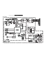
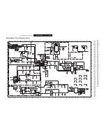
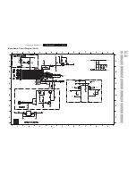
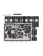
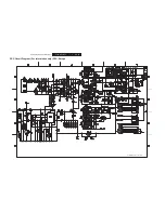
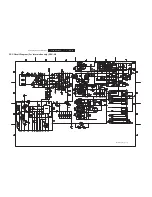
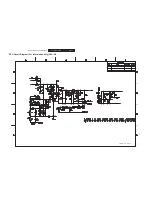
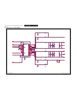
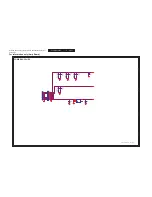
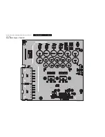
Mono Board: Circuit Diagram (Part 4)
7
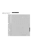
Circuit Diagram and PWB Layout
G4
0
3
2
VDD
VEE VSS
1
0
3
2
1
4X
0
3
0
1
M
AINL
MCLK
RST
1
0
AINR
GND REF_GND
VQ
LRCK
SCLK
FILT+
SDOUT
VL
VD
VA
OSCO
RDSCL
SCOUT
VREF
RDDA
QUAL
VDDD
VDDA
MPX
CIN
MODE
SYNC
TCON
OSCI
VSSA
VSSD
SDIN
SCLK
GND
VQ
FILT+
AOUTL
AOUTR
DEM
LRCK
MCLK
VA
D
E
F
G
H
I
1401 A1
1402 C1
1403 F1
1404 G1
1405 H1
1406 C9
2400 A9
2401 A9
2402 A8
2403 A9
2404 A10
2405 A14
2406 A2
2407 A10
2408 B12
2409 B2
2410 C6
1
2
3
4
5
6
7
8
9
10
11
12
13
14
1
2
3
4
5
6
7
8
9
10
11
12
13
14
A
B
C
D
E
F
G
H
I
A
B
C
# RDS
2411 C8
2412 C9
2413 D8
2414 D9
2415 D12
2416 D8
2417 D12
2418 D10
2419 D10
2420 D4
2421 E9
2422 E10
2423 E13
2424 E13
2425 E12
2426 E13
2427 E3
2428 E3
2429 E4
2430 E3
2431 E3
2432 F11
2433 F12
2434 F12
2435 F7
2436 F6
2437 F3
2438 F5
2439 G6
2440 G3
2441 G5
2442 G7
2443 H7
2444 H11
2445 H8
2446 H9
2447 H10
2448 H7
2449 H11
2450 H11
2451 H11
2452 I7
2453 I4
2454 I11
2455 I13
2456 I13
2457 I13
2458 I13
2459 I8
2460 I9
2461 I10
2462 H5
2463 I5
3400 A3
3401 A3
3402 A12
3403 A13
3404 A3
3405 A4
3406 A7
3407 A12
3408 A10
3409 B2
3410 B7
3411 B8
3412 B8
3413 B3
3414 B3
3415 B9
3416 B6
3417 C9
3419 C6
3420 C7
3421 C7
3422 C4
3423 D8
3424 D8
3425 D4
3426 D9
3427 D8
3428 D11
3429 D11
3430 D3
3431 D4
3432 E8
3433 E4
3434 E13
3435 E13
3436 E3
3437 E4
3438 E4
3439 E7
3440 F4
3441 F7
3442 F4
3443 F5
3444 F5
3445 G4
3446 G4
3447 G5
3448 G7
3449 G5
3450 H8
3451 H9
3452 H9
3453 H10
3454 H10
3455 H4
3456 H3
3457 H4
3458 H7
3459 H13
3460 I3
3461 I4
3462 I4
3463 I6
3464 I8
3465 I9
3466 I9
3467 I10
3468 I4
3469 I10
3470 I5
4400 C3
4401 D3
4402 D10
4403 E14
4404 H2
4405 H2
4406 H2
4407 I2
4408 H5
4409 I5
5400 A8
5401 D9
5402 I13
5407 I13
6400 A13
6401 A11
6403 C3
6404 C3
6405 D10
6406 I5
7400 A12
7401 A14
7402 A8
7403 B3
7405 C7
7406 D11
7407-1 H7
7407-2 I8
7408-1 H3
7408-2 I3
7409 H12
7410 I5
F400 A2
F401 A2
F402 A2
F403 A2
F404 A2
F405 A1
F406 A2
F407 A2
F408 B2
F409 B2
F410 C2
F411 C2
F412 D2
F413 D2
F414 D2
F415 E2
F416 F3
F417 G3
F418 G2
F419 H2
F420 H2
F421 H2
T400 B6
T401 C6
T402 D6
T403 E7
T404 E7
T405 H13
T406 I13
T407 H10
T408 I5
T409 I10
T410 A9
T411 A8
T412 B8
T413 B8
T414 E9
T415 E9
K
7
4
6
5
4
3
4401
4400
1
2
4
3
8
K
6
GND_A
GND_A
7
8
4
3465
LM833D
5
6
0
u
1
7407-2
GND_tu
2
2
4
2
10n
2406
D
2451
47u 25V
2449
47u 25V
F419
GND_A
+12AM
F407
3407
2K7
4409
T404
GND_A
2454
2444
22u 16V
16V
22u
GND_A
T406
p
2
2
8
5
4
2
2442
39p
p
0
2
2
1
6
4
2
8
3
4
2
p
0
0
1
GND_A
GND_A
GND_A
GND_A
T403
T402
T401
2
3
4
2
p
2
2
5
n
1
2459
2445
5
n
1
4408
D
1u0
2463
2462
1u0
4404
7408-1
2
6
1
BC847BS
1u0
F420
2436
1
4
4
2
p
0
0
1
33K
3452
9
4
4
3
K
2
2
K
2
2
4
4
4
3
3447
5K6
2413
-12AM
5K6
3443
1u0
GND_A
D
F406
GND_tu
GND_A
GND_A
0
6
4
2
p
0
2
2
p
0
2
2
7
4
4
2
6
4
4
2
p
0
2
2
p
2
2
3
3
4
2
GND_A
GND_A
GND_A
BC547B
2
3
1
3414
7403
D
1K5
2
K
2
7
1
4
3
p
2
8
2
1
4
2
F411
220K
3415
3410
2
6
4
3
K
0
2
2
1K0
GND_A
GND_A
GND_A
GND_A
T411
0
u
1
V
0
1
GND_tu
K
7
4
5
3
4
2
GND_tu
0
6
4
3
4
2
4
3
K
0
0
1
7407-1
3
2
1
8
4
GND_A
LM833D
2
0
4
4
GND_tu
6404
BZX384-C9V1
2400
100n
7
2
4
2
p
8
6
2429
1u0
4
13
6
3
11
GND_A
15
5
8
1
16
2
14
9
7
Φ
7406
CS5340
ADC
10
12
1
2
3
4
GND_A
GND_A
1402
B4B-EH-A
7
K
4
3
0
4
3
D
2439
3466
33K
1u0
K
2
2
2
0
4
3
7401
BC857B
BC857B
7400
3
2
4
2
n
0
1
4
2
4
2
2
u
2
0
u
1
0
1
4
2
V
0
1
5
2
4
3
15K
3453
K
6
5
GND_A
p
0
0
1
7
5
4
2
6
5
4
2
p
2
2
GND_A
GND_A
9
6
4
3
K
2
2
4
3
4
2
p
2
2
2420
GND_A
1
3
4
2
p
0
0
1
1u0
5
15
2
11
4
13
3
10
9
6
6
1
7
8
12
1
14
7405
HEF4052B
MDX
-12AM
GND_A
GND_A
+5VA
5402
600R
3455
680R
6400
BAS316
F408
3463
4K7
BC857B
1
3
2
2K2
0
1
4
7
3450
GND_A
2416
1u0
1K2
3427
1405
LPR6520-J920G
3
1
2
1
2
6
4
5
1403
LPR6520-J440G
3
T415
GND_A
100n
2443
3
1
2
GND_A
1404
LPR6520-J920G
5400
600R
GND_A
2401
TU_9V
GND_A
560p
0
3
4
2
p
8
6
3461
3437
5K6
470R
470R
3457
680R
3468
1
0
4
6
6
1
3
S
A
B
9
1
4
2
n
0
0
1
F418
2
u
2
2
0
4
2
0
4
4
2
p
8
6
p
8
6
7
3
4
2
1K0
GND_A
3406
1n0
2404
600R
5407
T408
GND_A
T405
15K
3467
V
6
1
GND_A
1
0
4
5
R
0
0
6
8
1
4
2
u
2
2
+12AM
GND_A
+12AM
F413
7
1
4
2
n
0
0
1
GND_A
F402
GND_A
2
3
4
5
6
7
8
9
10FE-BT-VK-N
1401
1
10
3464
F412
2K2
D
GND_A
8
K
6
1
4
4
3
F421
F404
9
1
4
3
8
K
6
F403
7
n
4
GND_A
1K2
1
2
4
2
3423
K
2
2
4
5
4
3
100R
3459
3
5
4
2
n
0
2
2
T414
D
GND_A
n
0
0
1
5
5
4
2
2
K
2
9
2
4
3
2
K
2
8
2
4
3
8
2
4
2
K
2
2
p
0
0
1
3
3
4
3
8
3
4
3
K
2
2
4K7
3430
3431
5K6
p
7
4
1
1
4
2
3401
1K2
1K2
D
3400
GND_A
D
2
u
2
V
5
2
u
7
4
8
0
4
2
n
0
0
1
5
2
4
2
5
1
4
2
9
0
4
3
4403
D
K
0
1
4M332
D
8
10
15
5
2
1
3
6
1
1
1406
7
9
4
13
14
1
2
16
7402
SAA6581T
Φ
3442
4K7
5K6
3416
2
2
4
3
K
6
5
D
GND_A
GND_A
D
4405
F415
GND_tu
F414
5
0
4
3
4
0
4
3
K
7
4
6
1
3
S
A
B
K
7
4
K
0
1
5
0
4
6
6
2
4
3
9
5
2450
100n
7
10
2
6
8
3
4
1
GND_A
Φ
CS4344
7409
F417
GND_A
F416
F401
F405
F400
120K
3448
D
6406
BAS316
39p
2452
-12AM
4R7
3413
u
0
1
9
0
4
2
3
0
4
6
6
1
3
S
A
B
T400
4407
4K7
3436
D
K
0
1
8
0
4
3
560p
2403
3440
5
3
4
560R
D
BC847BS
7408-2
V
5
2
u
0
0
1
5
0
4
2
GND_A
GND_A
D
GND_A
GND_A
GND_A
4K7
3446
5K6
3439
GND_A
GND_A
K
0
0
1
GND_A
GND_A
2
3
4
3
K
7
4
T410
+12VL
2
1
4
3
GND_A
GND_A
GND_A
T407
T409
K
7
4
D
4406
D
1
1
4
3
100n
2448
120K
33R
3458
3435
K
0
1
4
3
4
3
6
2
4
2
n
0
1
D
7
0
4
2
p
7
4
D
GND_A
T412
T413
0
2
4
3
8
K
6
GND_A
+12AM
7
n
4
4
1
4
2
3451
3470
22K
GND_A
560R
3445
-12AM
F409
F410
GND_A
GND_tu
TV_MUTE
I2C_CLK
I2C_DAT
MUTE
TU_RDS_IN
+5VL
DV33
RDS_DATA
RDS_CLK
+12AM
+12AM
DV33
TU_RDS_IN
DV33
AMP_RST
AUX_DATA_IN
PCM_MCLK
+5VA
PCM_LRCK
PCM_SCLK
PCM_SCLK
PCM_LRCK
PCM_MCLK
PCM_DATA4
SCART_LO_R
MUTE
SCART_LO_L
+5VL
MIC_L
-12AM
SCART_TV_Left_In
SCART_TV_Right_In
TU_9V
GND_tu
MIC
TU_SD
SEL_1
SEL_0
HTS3115_MB_SH4.pdf_2006_5_23


