background image

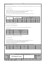
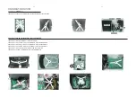
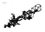
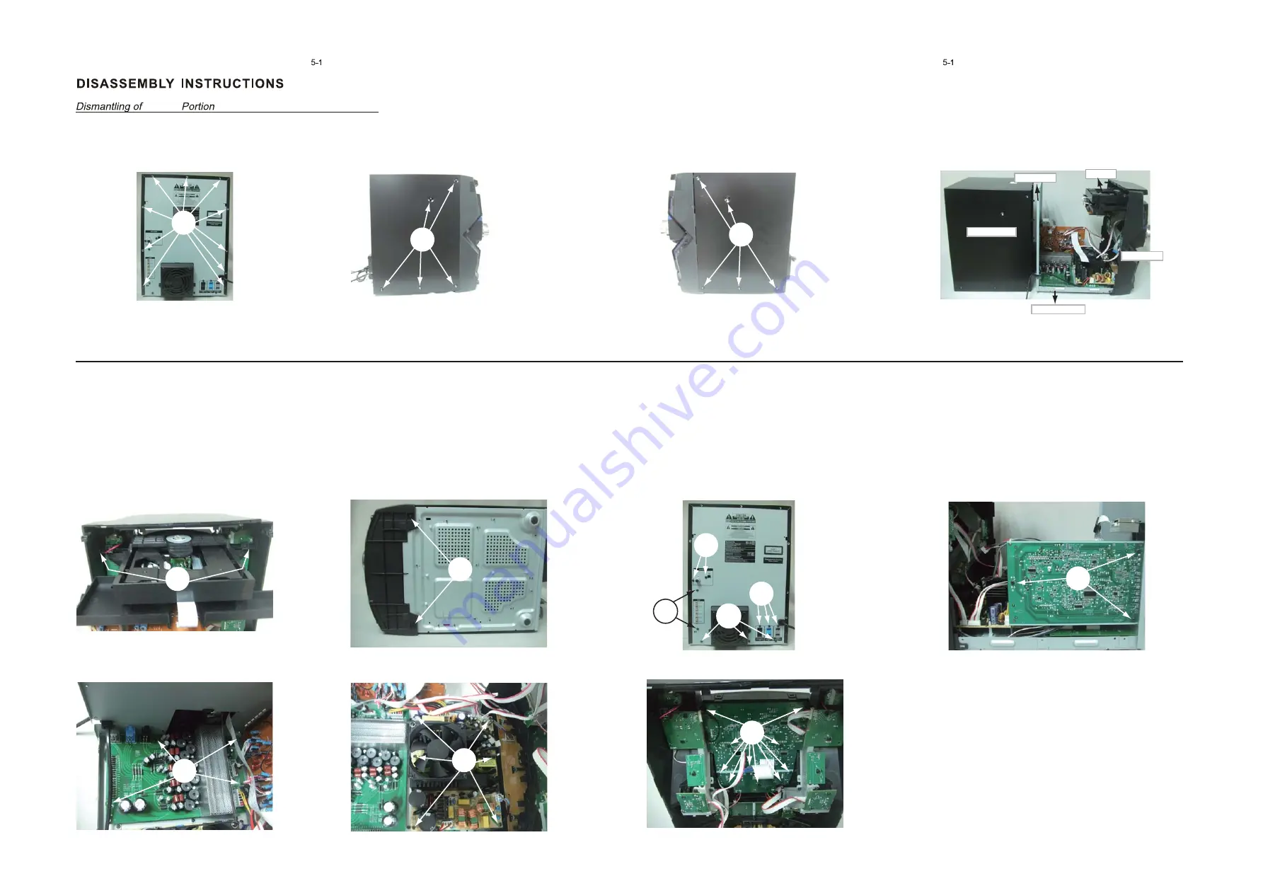
1)Remove 10 screws A and 10 screws B/C as indicated to loosen the outer plate.

Dismantling of the CD part and Bottom plate and PCB Board

OUTER

1)Remove 2 screws D as indicated to loosen the CD part.

2)Remove 2 screws E and 3 screws F as indicated to loosen the Bottom Plate.

4)Remove 2 screws G and 3 screws J as indicated to loosen the Main Board.

5)Remove 3 screws H and 4 screws K as indicated to loosen the Amp Board.

6)Remove 6 screws L as indicated to loosen the Smps power Board.

7)Remove 

10 screws M

 as indicated to loosen the Display Board.

A

B

C

REAR PLATE

FRONT CAB.

CD PART

OUTER PLATE

BOTTOM PLATE

D

E

H

I

G

F

J

K

L

M

Содержание FWT9200 Series

Страница 1: ... board Circuit diagram 11 1 Layout diagram 11 2 AMP board Circuit diagram 10 1 10 2 Layout diagram 10 3 Mechanical Exploded view 12 1 Copyright 2013 Philips Consumer Electronics B V Eindhoven The Netherlands All rights reserved No part of this publication may be reproduced stored in a retrieval system or transmitted in any form or by any means electronic mechanical photocopying or otherwise withou...

Страница 2: ...ATAM Mic BOARD MCU BOARD FWM9200 55 Tuner BOARD CD BOARD 55 Location of PC Boards Technical Specification and Connection Facilities C M C M C M C M C M C M ARGENTINA x 77 x 78 x 77 x 78 BRAZIL SMPS BOARD M C M C M C M C M C M C M C M C M C M C M C M C M C M C M M M C M C M C M C M C M C M CD PART Amp Board SMPS Board EQ Board MIC PC IN AUDIO IN Board MCU Board BT Board USB Board Display Board Ligh...

Страница 3: ... 63 7 21 1 5 3 57 8 2 6 1 63 7 21 1 5 3 57 8 2 6 1 63 7 21 1 5 3 57 2 7 0 5 63 7 21 1 5 3 57 86 6 DUG 63 7 21 1 5 3 57 781 5 63 7 21 OO 1 5 3 57 03 63 7 21 1 5 3 57 7 63 7 21 1 5 3 57 0LFURKRQH 63 7 21 1 5 3 57 9 56 21 29 59 63 7 21 Issue Andy Lai Checked DATE 2012 12 21 FWT9200 SH 190 content List 1 3 ...

Страница 4: ...eight inclusive packing 8 505KG 34 POWER ON OF MODE VOL 36 37 39 VFD DISPLAY 35 CABINET Diemensions with Boxes wxhxd 265mm X 382mm X 345mm Weight exclusive packing batery 26KG Units in Dealercarton DATE 11 A4 11 SH 190 1 NAME CHECK GENERAL PART 1 FRONT PANNEL SPECICFICATION Issued Date 21 Dec 12 30 31 32 ALBUM SERCH TUNING 33 STOP ALBUM SEARCH TUNING 38 29 28 USB LIGHT DISC IS USB DEL Finshing Chr...

Страница 5: ...5 DEPICTION Pos Description Page 7 FAN 1 2 3 4 5 7 8 6 9 10 11 12 13 10 14 Ver 1 2 3 FWT9200 All Version GENERAL PART 1 BACK PANNEL SPECICFICATION Issued Date Class No Weight exclusive packing batery 26Kg Units in Dealercarton Diemensions without Boxes wxhxd 1250mm X 340mm X 495mm Finshing Chrome Plate CABINET Diemensions with Boxes wxhxd 265mm X 382 mm X 345 mm Weight inclusive packing 8 5Kg Unit...

Страница 6: ...CO Power mode Without display 0 5W Ref to CRS 1 8 Prated NOM A INPUT 250W Maximum 1W DEMO mode OFF NOM A INPUT Standby with display 1W Ref to CRS Ref to CRS Voltage Selection Frequency POWER CONSUMPTION 12 05 55 77 78 98 61 93 37 10 3 6 9 CISPR 13 55 EN 60065 EN61000 3 2 EN61000 3 3 12 EN 60065 EN 55013 EN 55020 05 EN 55013 EN 55020 EN 60065 EN 60065 MODERATE climates N A till N A Degree SWITCH PO...

Страница 7: ...er L R 8 Ohm x2 at 40HZ to 100HZ Rear L R 4 Ohms X2 at 200Hz to 16 KHz Remarks OUTPUT POWER 1 At THD 10 Measured with 20Hz 20KHz filter Per Channel measuremend L R channel 360W Lim 1dB Power output RMS Power output RMS 1 Measurement output power just connect 1 channel loads Per channel measurement Tuner output Lim 6dB Rated Impedance FRONT L R 8 Ohms X2 at 40Hz to 16 KHz L R Subwoofer channel 360W...

Страница 8: ...UX as input source with the following set conditions 4 2 6 Inject sine wave 500mV at 1 KHz to L R channels of AUX IN socket Set DSC to JAZZ Flat mode and switch off DBB OPTIMAL 2 0 4 16 0 0 0 10 kHz host computer 0 For FWM998 Subwoofer in put 500mW 60HZ 3R Main computer Inject sine wave 500mV 2 4V to AUX IN socket with frequencies indicated in Table 1 60 Hz SUB Frequency DSC Modes with DBB Off JAZ...

Страница 9: ... 5 dB 0 dB The VEC modes are software controlled by switching the combination between DBB and DSC modes as show in Table 4 Set DSC to JAZZ Flat mode and switch of DBB OSM INCREDIBLE SURROUND Adjust volume level to obtain 1W across 3 OHM load at L R speaker output 15 dB Table 3 Tolerence 3 dB LEFT RIGHT LEFT RIGHT 60 Hz Max ON VEC MODE Optimal POP Jazz 10 kHz 1 Inject sine wave 2V to AUX IN socket ...

Страница 10: ...etting Clock and Timer LVSOD 7 SH 9 Volume at Wakeup Last Setting 1R RI 7LPHU 6HWWLQJV 1 ORFN FFXUDF Nom 1 sec day Limit 2 sec day TECHNIAL DESCRIPTION SOFTWARE IMPLEMENTED CLOCK TIMER FUNCTION WITH 12MHZ QUARTZ OSCILLATOR GENERAL PART 1 10 1 7256 Timer Wakeup Mode CD or Tuner or USB Remarks Time Setting 12hr for 37 version 24hrs for other version ...

Страница 11: ...lk 0 dB 1 KHz FWT9200 Frequency response 4 40HZ 16KHZ reference 1KHZ 40HZ 100HZ Reference 63HZ 200HZ 16KHZ Reference 1KHZ 45dB with 1 KHz filter 55dBA A weighted Description Channel Crosstalk 0 dB 1 KHz 45dB with 1 KHz filter Specification 3dB THD Noise 0dB 1Khz 2 Signal to Noise Ratio 0dB 1kHz A weighted 55dB A weighted Channel Crosstalk 0 dB 1 KHz 45dB 0 dB 1 KHz 45dB Measurement are directly do...

Страница 12: ...age Rejection IF Rejection 3 kHz 18 Crosstalk RF1mV Freq Dev 40kHz IF 10 7 450 IF 4 0 03 MHz Search Tuning Sensitivity ɲ26 10 dB 25 24 30 Stereo 46 dB Quieting 46 49 dBf Distortion RF 50mV M 80 3 5 INDICATORS VFD A M Nom Limit Unit Unit Amplification Reverse 2 4 dB AGC Figure of Merit 30 25 dB Distortion RF 1mV Frq Dev 75 kHz 2 3 WAVE RANGE TOLERANCE F M dB 3 dB Limiting Point 17 TUNING GRID Nom T...

Страница 13: ...equipment for measurement Test disc Fingerprint No audible defect TNO 11 of Sub chassis 8A Eccentric 150um 200um TNO 1 24 of 200um disc 7104 099 24960 Wedge mV dBA 4 dBA dB dB 600um 900um TNO 7 9 of SBC 444A 7104 099 24990 1 1 5 45dB 0 2 1 Playability acc To AR 30 05 239 Limit 3 1 Amplification reserve for CD 2dB 2dB Ref Level for CD is a 0dB track instead of a 6dB track REMARKS THD 10KHz 20dB 1 T...

Страница 14: ... Level Mobile Phone Distortion dB Channel Separation ı dB Level Diff f dB S N A weighted ı dBA S N Unweighted ı Frequency Response 125 16khz f dB Bluetooth at Module level Mobile Phone lim Unit Display N A ELECTRICAL DATA INDICATORS Bluetooth Flashing Yes Receive HSP N A Noise Reduction System No Bluetooth Version Ver2 1 EDR Receive A2DP N A 1 14 TECHNIAL DESCRIPTION Transmit A2DP N A Remote Contr...

Страница 15: ...1 5 mV dBA Microphone Power output RMS 550 20 mW 0 dB 1 KHz N A Signal to Noise Ratio 0dB 1kHz A weighted Channel Crosstalk 0 dB 63Hz N A Specification THD Noise 0dB 1Khz vol max 6 8 Output Voltage RL 33 k ohm dB 1 Khz N A Channel Unbalanceo about mic1 and mic2 Output Resistance N A 1 3 Nom Lim Unit GENERAL PART Measurement are directly done at the connector Microphone mic1 mic2 Description TECHNI...

Страница 16: ...ALCO Click Fit JST XH 2P Side 300 Ohm Dipole Loop Sagami 18 1uH 100kHz 10kHz No 75 Ohm Coaxial JST XH 2P Side 75 Ohm Pigtail Loop Sagami 18 1uH 230V 50Hz IEC IEC OVS EN60065 CLASS II SISR TAIWAN 79 AUST NZ EN60065 CLASS II 50kHz 9kHz 110 127V Switched 220 240V 50 60Hz No 05 12 EUROPE EN60065 SEMKO DEMKO NEMKO SEV BS415 UK EN55013 EN55020 No 75 Ohm Pigtail Loop Sagami 18 1uH 55 77 78 98 MAINS VOLTA...

Страница 17: ...llegato allo stesso potenziale che quello della massa dell apparecchio tramite un braccialetto a resistenza Assicurarsi che i componenti e anche gli utensili con quali si lavora siano anche a questo potenziale Pour votre sécurité ces documents doivent être utilisés par des spécia listes agréés seuls habilités à réparer votre appareil en panne GB Safety regulations require that the set be restored ...

Страница 18: ...perates properly after replacement if it was subject to electrostatic discharge during replacement its life might be shortened When replacing use a conductive mat soldering iron with ground wire etc to protect the laser diode form damage by static electricity And also the LSI and IC are same as above Soldering iron with ground wire or ceramic type Ground conductive wrist strap for body Conductive ...

Страница 19: ...sts the fault must be located and corrected Repeat the above test with the DVD VIDEO PLAYER power plug reversed NEVER RETURN A DVD VIDEO PLAYER TO THE CUSTOMER WITHOUT TAKING NECESSARY CORRECTIVE ACTION READING SHOULD NOT EXCEED 0 3V DVD VIDEO PLAYER AC OUTLET AC VOLTMETER Test all exposed metal Voltmeter Hook up for Leakage Current Check 0 15uF 150V AC 1500 10W 5000 per volt or more sensitivity G...

Страница 20: ...ealing edge is very flimsy Don t bend or fold sealing edge 2 2 3 Folding edge The folding edge is formed in battery process and has passed all hermetic tests Don t open or deform folding edge 2 2 4 Tabs The battery tabs are not so rigid especially for aluminum tab Don t bend tab 2 2 5 Mechanical shock Don t fall hit bend battery body 2 2 6 Short Short terminals of battery is strictly prohibited it...

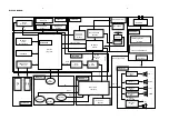
Страница 21: ...IC MUL L R IIC PCM BCK LRCK DATE PCM CD L R TUNER L R CONTROL DATA CD PCM BCK LRCK DATE TDA8954 1 SE FUNCTION IC TDA7468D 3CD LOADER TDA8954 1 BTL SUB R 2 150W 1 300W USB2 PLAY LED DRIVER BU2090F IIC MP3 LINE USB CHANGE FFE1 1S CD DOOR MOTOR SWITCH POWER SUPPLY DC 39V Main Supply Voltage support Dock DCK3060 AC CORD CD Board MCU Board MIC Board USB Board AMP Board MAIN Board POWER Board VFD Displa...

Страница 22: ...WIRING DIAGRAM 4 1 4 1 ...

Страница 23: ...rews E and 3 screws F as indicated to loosen the Bottom Plate 4 Remove 2 screws G and 3 screws J as indicated to loosen the Main Board 5 Remove 3 screws H and 4 screws K as indicated to loosen the Amp Board 6 Remove 6 screws L as indicated to loosen the Smps power Board 7 Remove 10 screws M as indicated to loosen the Display Board A B C REAR PLATE FRONT CAB CD PART OUTER PLATE BOTTOM PLATE D E H I...

Страница 24: ......

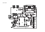
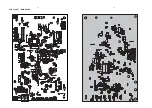
Страница 25: ...6 2 6 2 PCB LAYOUT MAIN BOARD ...

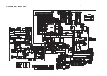
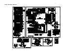
Страница 26: ...7 1 7 1 CIRCUIT DIAGRAM DISPLAY BOARD ...

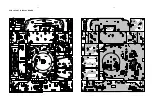
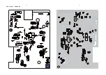
Страница 27: ...PCB LAYOUT DISPLAY BOARD 7 2 7 2 ...

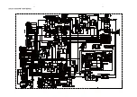
Страница 28: ...G2 7 G3 8 GND 16 VCC 15 OE 14 G4 13 G5 12 G6 11 G7 10 QS1 9 QS2 IC505 74HC4094 R588 100R R577 0R C578 220u 16 Q523 AO3401A C565 104 R582 100k R584 2K2 3 1 2 Q522 BC817 25 3 1 2 Q501 BC807 25 C568 104 R528 10k C534 470P C533 470P C535 3U3 50v C536 3U3 50v R537 3K3 R536 3K3 R531 2K2 R533 2K2 C531 470P C532 470P R534 2K2 R535 2K2 R521 10K R541 10K 5 4 3 2 6 1 1 2 3 4 5 6 CON521 6P2 0MM 90C 1 VINFC 2 ...

Страница 29: ...8 2 8 2 PCB LAYOUT CD BOARD ...

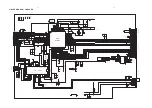
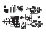
Страница 30: ...CIRCUIT DIAGRAM MCU BOARD 9 1 9 1 ...

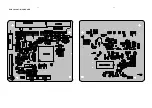
Страница 31: ...PCB LAYOUT MCU BOARD 9 2 9 2 ...

Страница 32: ...3 VDDA 4 IN2 5 IN2 6 MODE 7 OSC 8 IN1 9 IN1 10 DIAG1 11 OSCREF 12 DIAG2 13 PROT 14 VDDP1 15 BOOT1 16 OUT1 17 VSSP1 18 STAB1 19 NC 20 VSSP2 21 OUT2 22 BOOT2 23 VDDP2 24 VSSD U702 TDA8954TH C785 104 C787 104 C786 104P C784 15N C783 15N R761 10R R762 10R C790 220P C792 220P C796 100N R765 22R C798 100N R763 22R L703 15UH L704 15UH C781 104P C780 104 C782 104 C778 224 C779 47PF C777 473 C776 220N D707...

Страница 33: ...4 U707 A D4556 6 5 7 8 U707 B R776 NC C7105 224 R771 47K R770 10K C7112 474 R780 5 6K C7111 474 R779 5 6K R777 220 R778 220 C7110 330PF R781 8k2 C7113 330PF R782 1K C7190 330PF 1 VSSA 2 SGND 3 VDDA 4 IN2 5 IN2 6 MODE 7 OSC 8 IN1 9 IN1 10 DIAG1 11 OSCREF 12 DIAG2 13 PROT 14 VDDP1 15 BOOT1 16 OUT1 17 VSSP1 18 STAB1 19 NC 20 VSSP2 21 OUT2 22 BOOT2 23 VDDP2 24 VSSD U705 TDA8954TH C7191 330PF C7202 104...

Страница 34: ...PCB LAYOUT AMP BOARD 10 3 10 3 ...

Страница 35: ...CIRCUIT DIAGRAM TUNER BOARD 11 1 11 1 ...

Страница 36: ...PCB LAYOUT TUNER BOARD 11 2 11 2 ...

Страница 37: ...12 1 12 1 EXPLODED VIEW ...

Отзывы: