background image

LAYOUT DIAGRAM - CASSETTE BOARD

COPPER SIDE VIEW

7 - 3

7 - 3 

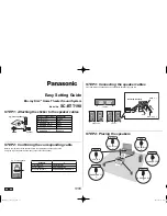
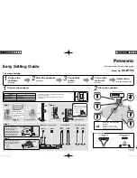
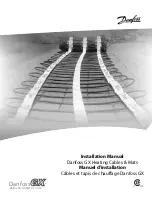
Содержание FWD154/98

Страница 1: ...the prior permission of Philips CONTENTS Technical specification 1 2 Service measurement setup 1 3 Service aids 1 4 Instructions on CD playability 2 1 2 2 Disassembly diagram 3 1 Block diagram 4 1 Wiring diagram 4 2 Display board Circuit diagram 5 1 5 3 Layout diagram 5 4 5 5 AMP board Circuit diagram 6 1 Layout diagram 6 2 6 3 Cassette board Circuit diagram 7 1 Layout diagram 7 2 7 3 USB Line in ...

Страница 2: ...Type Semiconductor Disc Diameter 12cm 8cm Video Decoding MPEG 2 MPEG 1 Video DAC 10 Bits Signal System PAL NTSC Video Format 4 3 16 9 Video S N 56 dB minimum Composite Video Output 1 0 Vp p 75 ohm Audio DAC 24Bits 96 kHz Total Harmonic Distortion 1 Frequency Response 4 Hz 20 kHz 44 1 kHz 4 Hz 22 kHz 48 kHz 4 Hz 44 kHz 96 kHz Total harmonic distortion 0 1 1 kHz Channel separation 40 dB minimum 1 kH...

Страница 3: ...15kHz e g 7122 707 48001 LF Voltmeter e g PM2534 DUT S N and distortion meter e g Sound Technology ST1700B Frame aerial e g 7122 707 89001 Tuner AM MW LW To avoid atmospheric interference all AM measurements have to be carried out in a Faraday s cage Use a bandpass filter or at least a high pass filter with 250Hz to eliminate hum 50Hz 100Hz RF Generator e g PM5326 Ri 50 Bandpass 250Hz 15kHz e g 71...

Страница 4: ...ng make sure that you are connected with the same potential as the mass of the set via a wrist wrap with resistance Keep components and tools also at this potential ESD CLASS 1 LASER PRODUCT GB Safety regulations require that the set be restored to its original condition and that parts which are identical with those specified be used Safety components are marked by the symbol Lead free ...

Страница 5: ...T OK check playability N Y playability ok check playability check playability return set Customer complaint CD related problem fast lens cleaning 1 2 3 For flap loaders access to CD drive possible cleaning method 4 is recommended INSTRUCTIONS ON CD PLAYABILITY 2 1 Exchange CDM 1 4 For description see following pages ...

Страница 6: ...viously caused by a scratched dirty or copy protected CD In case problems remain the customer is requested to contact the workshop directly The lens cleaning method 3 should be mentioned in the addendum sheet The final wording in national language as well as the printing is under responsibility of the Regional Service Organizations 4 LIQUID LENS CLEANING Because the material of the lens is synthet...

Страница 7: ...PEN CLOSE to open CD door b Pull out CD door c Press OPEN CLOSE button to close the CD tray power off the mainset and unplug the AC power cord 4 Remove top cabinet 5 Loosen 2 screws PA3x18 to remove CD tray 6 Loosen 6 screws T3 10 and 14 screws PT3x10 to remove Main board 1 2 3 4 5 6 8 7 3 Loosen 6 screws BT3 12 in rear cabinet CD DOOR 1 2 1 2 3 4 5 6 1 2 3 PT 3x6螺 ...

Страница 8: ...VO AMPLIFIER 4558 TDA8948 INPUT OUTPUT TERMINALS AUX LINE IN USB PORT YUV S VHS CVB COAXIAL HEADPHONE TU_VCC 9V PWR_VCC VCC_ 5V MCU_VCC 3 3V MCU_VCC 3 3V M 5V AU_VCC 30V AU_VCC POWER MANAGEMENT 12V 30V MCU_VCC 3 3V VCC_ 5V USB_ 5V PWR_VCC 9V TU_VCC 9V AU_VCC 9V USB_ 5V SPHE8202LQ PIC18F44J10 D5888S TDA8947 x 2 PT7312 LV23010 120V 240V SET BLOCK DIAGRAM 4 1 4 1 ...

Страница 9: ...SET WIRING DIAGRAM 4 2 4 2 ...

Страница 10: ...5 1 5 1 CIRCUIT DIAGRAM DISPLAY BOARD EQ VOL PART ...

Страница 11: ...CIRCUIT DIAGRAM DISPLAY BOARD LCD PART 5 2 5 2 ...

Страница 12: ...CIRCUIT DIAGRAM DISPLAY BOARD MCU PART 5 3 5 3 ...

Страница 13: ...LAYOUT DIAGRAM DISPLAY BOARD COMPONENT SIDE VIEW 5 4 5 4 ...

Страница 14: ...LAYOUT DIAGRAM DISPLAY BOARD COPPER SIDE VIEW 5 5 5 5 ...

Страница 15: ...CIRCUIT DIAGRAM AMP BOARD 6 1 6 1 ...

Страница 16: ...LAYOUT DIAGRAM AMP BOARD COMPONENT SIDE VIEW 6 2 6 2 ...

Страница 17: ...LAYOUT DIAGRAM AMP BOARD COPPER SIDE VIEW 6 3 6 3 ...

Страница 18: ...CIRCUIT DIAGRAM CASSETTE BOARD Cassette is not repaired diagram for referrence only 7 1 7 1 ...

Страница 19: ...LAYOUT DIAGRAM CASSETTE BOARD COMPONENT SIDE VIEW 7 2 7 2 ...

Страница 20: ...LAYOUT DIAGRAM CASSETTE BOARD COPPER SIDE VIEW 7 3 7 3 ...

Страница 21: ...8 1 8 1 CIRCUIT DIAGRAM USB LINE IN VIDEO OUT BOARD ...

Страница 22: ...8 2 8 2 LAYOUT DIAGRAM USB LINE IN VIDEO OUT BOARD ...

Страница 23: ...CIRCUIT DIAGRAM DVD BOARD DVD is not repaired diagram for referrence only 9 1 9 1 ...

Страница 24: ...CIRCUIT DIAGRAM DVD BOARD DVD is not repaired diagram for referrence only 9 2 9 2 ...

Страница 25: ...CIRCUIT DIAGRAM DVD BOARD DVD is not repaired diagram for referrence only 9 3 9 3 ...

Страница 26: ...CIRCUIT DIAGRAM DVD BOARD DVD is not repaired diagram for referrence only 9 4 9 4 ...

Страница 27: ...LAYOUT DIAGRAM DVD BOARD DVD is not repaired diagram for referrence only 9 5 9 5 ...

Страница 28: ...EXPLODED VIEW DIAGRAM 10 1 10 1 17 27 28 29 30 31 32 36 35 19 33 25 20 26 22 24 18 40 23 45 21 49 42 41 46 16 PCB4 48 43 ...

Страница 29: ...EAR STAND MODE 0 8 37 996500038818 RECORD SPRING 38 996510021221 CASS DOOR SPING D0 8mm 39 996510002265 FWM185 CASS KEYS DOOR SPRING 40 996510022843 LCD BRACKET 41 994000004736 SLIDE SWITCH SSV 12 8700S 42 996510022765 REAR CABINET 43 996510022759 DVD MECH SONY KHM 313AAD 44 996510022768 24 PIN FFC FLAT FLEXIBLE CABLE 45 996510022756 DVD LOADER COMPLETED WXD 8213 46 996510022766 TRANSFORMER UL EML...

Страница 30: ...CD DRIVER 48P VR301 996510018244 ENCODER EC121102X2B HA1 137 XT301 996500038822 CRYSTAL JF32 768kHz JU2x6 XT302 996500038823 CRYSTAL 8MHz HC 49US AMP BOARD ASSEMBLY F501 994000004782 FUSE 50T D5X20 1 6A 250V S B F502 996510002287 FUSE T6 3A 250V 5x20 IC501 996510009066 IC TDA8948J DBS17P PHILIPS IC503 996510002294 IC D4558 SOP8 Q501 996510021217 TR PNP 2SB1274 TO 220F EP Q502 996510021406 MOSFET T...

Отзывы: