PCS 102 791
12-3
12-3
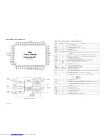
PIN DESCRIPTION
Name
Number
I/O
Definition
VSS
1,25:26,31,72,75,77,91,100
I
Ground.
VCC
5,16,32,66,73,78,90
I
Voltage supply, 5 V.
DSC_C
6
I
Clock for programming to access internal registers.
AUX0
7
I/O
Servo Forward or Control Pin.
AUX1
9
I/O
Servo Reverse or Control Pin.
AUX2
11
I/O
Servo LDON or Control Pin.
AUX3
70
I/O
Servo CW/Limit or Control Pin.
AUX4
69
I/O
Servo CCW/Close or Control Pin.
AUX5
68
I/O
Servo Data or Control Pin.
AUX6
67
I/O
Servo XLAT or Control Pin/VFD_DO.
AUX7
14
I/O
Servo BRKM/Sense or Control Pin/VFD_DI.
AUX8
18
I/O
Servo Mute/Open or Control Pin/VFD_CLK.
AUX9
20
I/O
Servo SQS0 or Control Pin.
AUX10
34
I/O
Servo SQCK or Control Pin.
AUX11
35
I/O
3880 IRQ or Interrupt Output or Control Pin.
AUX12
36
I/O
CD C2PO or Interrupt Input or Control Pin.
AUX13
38
I/O
Serial Interrupt/CD-Mute or Control Pin.
AUX14
39
I/O
Servo SCOR (S0S1) or Interrupt Input or Control Pin.
AUX15
40
I/O
Interrupt Input or Control Pin.
DSC_D[7:0]
81,83,85,93,95,97,99,8
I/O
Data for programming to access internal registers.
DSC_S
10
I
Strobe for programming to access internal registers.
DCLK
12
O
Dual-purpose pin DCLK is the MPEG decoder clock.
EXT_CLK
I
EXT_CLK is the external clock EXT_CLK is an input during bypass PLL mode.
RESET_B
13
I
Video reset (active-low).
MUTE
15
O
Audio mute.
MCLK
17
I
Audio master clock.
TWS
19
I
Dual-purpose pin TWS is the transmit audio frame sync.
SPLL_OUT
O
SPLL_OUT is the select PLL output.
TSD
21
I
Transmit audio data input.
TBCK
22
I
Transmit audio bit clock.
RWS
23
O
Dual-purpose pin RWS is the receive audio frame sync.
SEL_PLL1
I
Pins SEL_PLL[1:0] select the PLL clock frequency for the DCLK output.
RSTOUT_B
24
O
Reset output (active-low).
NC
2:4,27:30,76
No connect. Do not connect to these pins.
RSD
33
O
Dual-purpose pin. RSD is the receive audio data input.
SEL_PLL0
I
SEL_PLL0 along with SEL_PLL1 select the PLL clock frequency for the DCLK output. See the
table for pin number 23.
RBCK
37
O
Dual-purpose pin. RBCK is the receive audio bit clock.
SER_IN
I
SER_IN is the serial input DSC mode.
0 - Parallel DSC mode.
1 - Serial DSC mode.
VSSAA
41,51
I
Audio Analog Ground.
VCM
42
I
ADC Common Mode Reference (CMR) buffer output. CMR is approximately 2.25 V. Bypass to
analog ground with 47 mF electrolytic in parallel with 0.1 mF.
VREFP
43
I
DAC and ADC maximum reference. Bypass to VCMR with 10 mF in parallel with 0.1 mF.
VCCAA
44
I
Analog VCC, 5 V.
AOR+, AOR-
45:46
O
Right channel output.
AOL-, AOL+
47:48
O
Left channel output.
MIC1
49
I
Microphone input 1.
MIC2
50
I
Microphone input 2.
VREF
52
I
Internal resistor divider generates Common Mode Reference (CMR) voltage. Bypass to ana-
log ground with 0.1 mF.
VREFM
53
I
DAC and ADC minimum reference. Bypass to VCMR with 10 mF in parallel with 0.1 mF.
RSET
54
I
Full scale DAC current adjustment.
COMP
55
I
Compensation pin.
VSSAV
56:57,62:63
I
Video Analog Ground
CDAC
58
O
Modulated chrominance output.
VCCAV
59,60
I
Video VCC, 5 V
YDAC
61
O
Y luminance data bus for screen video port.
VDAC
64
O
Composite video output.
ACAP
65
I
Audio CAP
XOUT
71
O
Crystal output.
XIN
74
I
27 MHz crystal input.
PCLK
79
I/O
13.5 MHz pixel clock.
2XPCLK
80
I/O
27 MHz (2 times pixel clock).
HSYN_B
82
O
Horizontal sync (active-low).
VSYN_B
84
O
Vertical sync (active-low).
YUV[7:0]
86:89,92,94,96,98
I
YUV data bus for screen video port.
Name
Number
I/O
Definition
SEL_PLL1
SEL_PLL0
DCLK
0
0
Bypass PLL (input mode)
0
1
27 MHz (output mode)
1
0
32.4 MHz (output mode)
1
1
40.5 MHz (output mode)
1
MIC2
MIC1
AOL+
AOL-
AOR-
AOR+
VCCAA
VREFP
VCM
VSSAA
AUX15/IR
AUX14/SOS1
AUX13/SP
RBCK/SER_IN
AUX12/C2PO
AUX11/IRQ
AUX10/SQCK
RSD/SEL_PLL0
VCC
VSS
DSC_D7
HSYN_B
DSC_D6
VSYN_B
DSC_D5
YUV7
YUV6
YUV5
YUV4
VCC
VSS
YUV3
DSC_D4
YUV2
DSC_D3
YUV1
DSC_D2
YUV0
DSC_D1
VSS
TS
D
AUX
9
/S
QS
0
TW
S
/SP
L
L
_OU
T
AU
X
8
/V
FD
_
C
LK
MC
LK
VC
C
MU
T
E
AUX7
/V
F
D
_
D
I
RES
ET
_
B
DCL
K
/EX
T_
CL
K
AU
X2
DSC
_
S
AU
X1
DSC_
D0
AU
X0
DS
C_
C
VC
C
NC
NC
VSS
NC
NC
NC
NC
NC
VSS
VSS
RST
OUT
_
B
RW
S
/SE
L_P
LL1
TB
C
K
YD
A
C
V
SSA
V
V
SSA
V
VD
A
C
AC
A
P
VC
C
AU
X
6
/V
FD
_
D
O
AU
X
5
AU
X
4
AU
X
3
XO
U
T
VS
S
VC
C
XI
N
VS
S
NC
VS
S
VC
C
PC
L
K
2X
P
C
LK
V
SSA
A
VR
E
F
VR
E
F
M
R
SET
CO
M
P
V
SSA
V
V
SSA
V
CD
A
C
V
CCA
V
V
CCA
V
31
30
51
50
80
81
100
2
3
4
5
6
7
8
9
10 11 12 13 14 15 16 17 18 19 20 21 22 23 24 25 26 27 28 29
49
48
47
46
45
44
43
42
41
40
39
38
37
36
35
34
33
32
79 78 77 76 75 74 73 72 71 70 69 68 67 66 65 64 63 62 61 60 59 58 57 56 55 54 53 52
82
83
84
85
86
87
88
89
90
91
92
93
94
95
96
97
98
99
Visba ES3883
Video CD
Companion Chip
ES3883 VIDEO CD COMPANION CHIP


