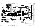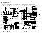
stage .7
11-1
11-1
TABLE OF CONTENTS
Brief Circuit Description.........................................................................11-1
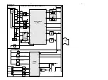
Block Diagram.......................................................................................11-3
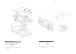
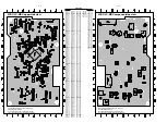
Component Layout
Mains part
.............................................................11-4
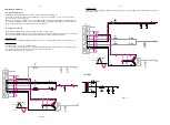
Circuit Diagram
Mains part
..................................................................11-5
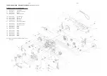
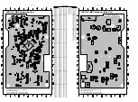
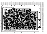
Component Layout
Power part
............................................................11-6
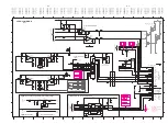
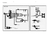
Circuit Diagram
Power part
..................................................................11-7
Circuit details:
Amplifier:
Attention:
In the POWER 2001 module the power amplifier IC AN7591 is used as a bridge-amplifier.
Any connection from output to ground will destroy the outpout stages!
•
Via the AMP_ON control line, connected to pins 6 (Stby), the power amplifiers are switched on/off by the µP.
High level (approx. 4,5V): power amplifiers switched on
Low level (approx. 0V): power amplifiers switched off
•
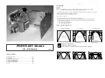
Super class G - operation
The power amplifiers operate as so-called super class G - amplifiers:
The supply pins 12 (Vcc) are not just connected to one fixed DC-supply as in conventional amplifiers.
Dependent on the output power there are three different DC-voltages supplied to the power amplifiers:
⇒
+C1 (+20V) for low output power
⇒
+B1 (+29V) for medium output power
⇒
+A1 (+41V for high output power
Principle / benefit of Super Class G
Conventional power stage
Class G amplifier
Super class G amplifier
output signal
output signal
output signal
+A
+B
+C
+C
+A
+B
+C
Voltage drop on power stage IC
Voltage drop on switching transistor(s)
Benefit - voltage drop on switching transistor(s) reduces total power dissipation
activating point +A
activating point +B
activating point +A
Po
w
e
r
Power
dissipation
Po
w
e
r
Power
dissipation
Po
w
e
r
Power
dissipation
Output power
Benefit
Output power
%
%
%
Output power
Benefit
+C
+A
+A
+C
+A
+B
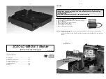
POWER 2001 Module
(30 - 70W Version)

