background image

1-8-5

E5P31TR

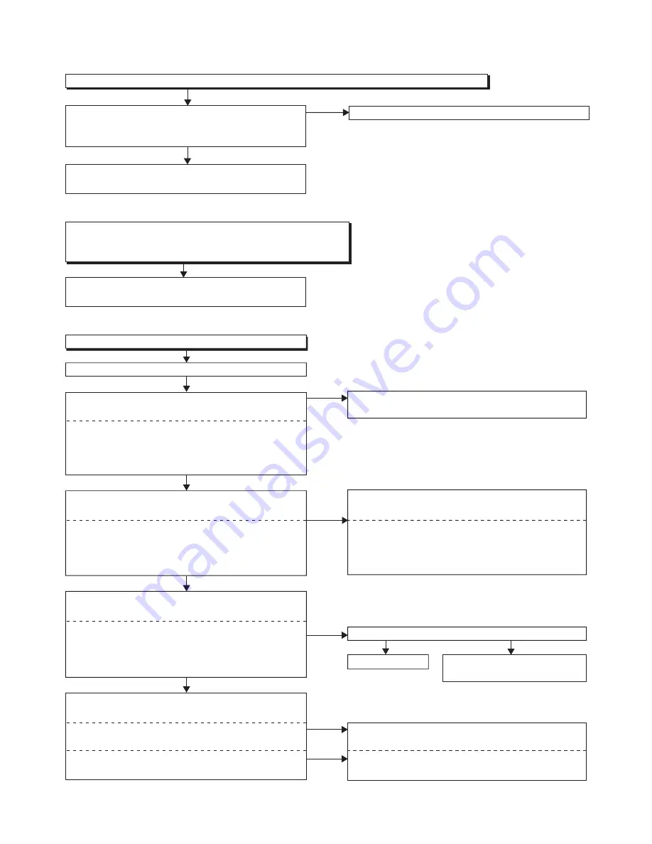
Is 5V voltage supplied to the Pin(13) of IC2300?

Replace IC2300.

Check P-ON+5V line and
service it if detective.

Are the video signals outputted to each pin of 
IC2300?

Yes

No

Yes

Yes

No

IC2300   12PIN    VIDEO-Y(I/P)
IC2300   10PIN    VIDEO-Pb/Cb
IC2300     9PIN    VIDEO-Pr/Cr
IC2300   14PIN    VIDEO

Check the periphery of JK2300 from Pin(9,10,12) 
of IC2300 and service it if detective.

Check the periphery of JK2300 from Pin(14) of 
IC2300 and service it if detective.

Are the video signals outputted to the specific 
output terminal?

Are the component video signals outputted to the 
VIDEO OUT terminal (JK2300)?

No

No

Are the composite video signals outputted to 
the VIDEO OUT terminal (JK23 00)?    

FLOW CHART NO.19

Picture does not appear normally. 

Set the disc on the disc tray, and playback.

Are the video signals outputted to each pin of 
CN2200?

Replace the BD Main CBA & BD Mechanism 
Assembly.

Check the line between each pin of CN2200 and 
each pin of IC2300, and service it if detective.

CN2200  13PIN 

 IC2300    1PIN   VIDEO

CN2200  11PIN 

 IC2300    3PIN   VIDEO-Y(I/P)

CN2200    9PIN 

 IC2300    4PIN   VIDEO-Pb/Cb

CN2200    7PIN 

 IC2300    5PIN   VIDEO-Pr/Cr

Are the video signals shown above inputted into 
each pin of IC2300?

Yes

No

No

CN2201   13PIN    VIDEO
CN2201   11PIN    VIDEO-Y(I/P)
CN2201     9PIN    VIDEO-Pb/Cb
CN2201     7PIN    VIDEO-Pr/Cr

IC2300     1PIN    VIDEO
IC2300     3PIN    VIDEO-Y(I/P)
IC2300     4PIN    VIDEO-Pb/Cb
IC2300     5PIN    VIDEO-Pr/Cr

Yes

FLOW CHART NO.18

The disc tray cannot be opened and closed. 
[No Disc] indicated. 
Both functions of picture and sound do not operate normally. 

Replace the BD Main CBA & BD Mechanism  
Assembly.

Yes

FLOW CHART NO.17

The disc tray cannot be opened and closed. (It can be done using the remote control unit.)

Is the normal control voltage inputted to Pin(30) of 
IC2000? Refer to "FLOW CHART NO.15" <The key 
operation is not functioning.>

Replace the BD Main CBA & BD Mechanism  
Assembly.

Replace the "OPEN/CLOSE" switch (SW6004).

No

Содержание BDP3010/F8 C

Страница 1: ...SERVICE MANUAL BLU RAY DISC PLAYER BDP3010 F8 BDP3010 F8 C ...

Страница 2: ...s consequences of each way Consequently P F has not undertaken any such broad evaluation Accordingly a servicer who uses a service procedure or tool which is not recommended by P F must first use all precautions thoroughly so that neither his safety nor the safe operation of the equipment will be jeopardized by the service method selected TABLE OF CONTENTS Specifications 1 1 1 Laser Beam Safety Pr...

Страница 3: ...1 1 1 E5P32SP SPECIFICATIONS ...

Страница 4: ...way from the pickup lens when the diode is turned on Do not look directly at the laser beam CAUTION Use of controls and adjustments or doing procedures other than those specified herein may result in hazardous radiation exposure Location Inside Top of BD mechanism Do not look directly at the laser beam coming from the pickup or allow it to strike against your skin Drive Mechanism Assembly Laser Be...

Страница 5: ...cal for safety Replace only with part number specified B In addition to safety other parts and assemblies are specified for conformance with regulations applying to spurious radiation These must also be replaced only with specified replacements Examples RF converters RF cables noise blocking capacitors and noise blocking filters etc C Use specified internal wiring Note especially 1 Wires covered w...

Страница 6: ...le parts RF terminals antenna terminals video and audio input and output terminals microphone jacks earphone jacks etc is lower than or equal to the specified value in the table below Measuring Method Power ON Insert load Z between B earth ground power cord plug prongs and exposed accessible parts Use an AC voltmeter to measure across the terminals of load Z See Fig 2 and the following table Table...

Страница 7: ...achine then apply hot air to the Flat Pack IC about 5 to 6 seconds Fig S 1 1 2 Remove the flat pack IC with tweezers while applying the hot air 3 Bottom of the flat pack IC is fixed with glue to the CBA when removing entire flat pack IC first apply soldering iron to center of the flat pack IC and heat up Then remove glue will be melted Fig S 1 6 4 Release the flat pack IC from the CBA using tweeze...

Страница 8: ...by one using a sharp pin or wire to which solder will not adhere iron wire When heating the pins use a fine tip soldering iron or a hot air desoldering machine Fig S 1 4 3 Bottom of the flat pack IC is fixed with glue to the CBA when removing entire flat pack IC first apply soldering iron to center of the flat pack IC and heat up Then remove glue will be melted Fig S 1 6 4 Release the flat pack IC...

Страница 9: ... Fig S 1 6 Note When using a soldering iron care must be taken to ensure that the flat pack IC is not being held by glue When the flat pack IC is removed from the CBA handle it gently because it may be damaged if force is applied 2 Installation 1 Using desoldering braid remove the solder from the foil of each pin of the flat pack IC on the CBA so you can install a replacement flat pack IC more eas...

Страница 10: ...ed to remove any static electricity that may be charged on the body 2 Ground for Workbench Be sure to place a conductive sheet or copper plate with proper grounding 1 MΩ on the workbench or other surface where the semi conductors are to be placed Because the static electricity charge on clothing will not escape through the body grounding band be careful to avoid contacting semi conductors with you...

Страница 11: ... 5 Refer to Reference Notes Reference Notes 1 CAUTION 1 Locking Tabs L 1 L 2 and L 3 are fragile Be careful not to break them 2 The BD Main CBA BD Mechanism Assembly is adjusted as a unit at factory Therefore do not disassemble it Replace the BD Main CBA BD Mechanism Assembly as a unit ID Loc No Part Removal Fig No Remove Unhook Unlock Release Unplug Desolder Note 1 Top Cover D1 6 S 1 2 Front Asse...

Страница 12: ...bly L 1 L 3 L 2 CN6000 L 1 Fig D2 4 Rear Panel S 1 S 4 S 2 S 3 Fig D3 5 BD Main CBA BD Mechanism Assembly 6 Main PCB Bracket CN7101 S 5 S 7 CN6101 S 6 See Reference Notes 2 Fig D4 9 AV CBA 8 Power Holder Hook CN2004 S 8 7 Motor DC Fan Fig D5 ...

Страница 13: ...1DC 3 How to Eject Manually 1 Remove the Top Cover Front Assembly and BD Main CBA BD Mechanism Assembly 2 Slide the portion A in the direction of the arrow 3 Pull the tray out manually and remove a disc Portion A ...

Страница 14: ...on the remote control unit in that order Fig a appears on the screen All VFD lights Fig a 4 Press C button on the remote control unit Fig b appears on the screen and Fig c appears on the VFD Fig b Fig c 5 To exit this mode press button differ depending on the models F W Name Version Region Pickup Version Info EXIT POWER EEPROM CLEAR STOP differ depending on the models F W Name Version Region Picku...

Страница 15: ...ollows Fig e Version Up Mode Fig f VFD in Version Up Mode 5 After programming is finished the checksum on the VFD Fig g Fig g VFD upon Finishing the Programming Mode Exampl Checksum appears on the VFD then the tray will open automatically Remove the disc on the tray At this time no button is available 6 Unplug the AC cord from the AC outlet Then plug it again 7 Turn the power on differ depending o...

Страница 16: ...e disc on the tray and close the tray 3 Press 1 2 3 4 and INFO buttons on the remote control unit in that order Fig h appears on the screen Fig h 4 To exit this mode press button differ depending on the models F W Name Version Region Pickup Version Info EXIT POWER EEPROM CLEAR STOP ...

Страница 17: ...nd Fig i appears on the VFD Fig h Fig i VFD in Update Mode 8 GOODBYE on the VFD and turn the power off automatically when it finishes 9 The power turns on and the tray will open automatically Remove the disc on the tray All the item of SETUP are initialized Software Upgrade Please insert a disc for software Upgrade If you want to exit Upgrade press BACK Software Upgrade Loading Disc Software Upgra...

Страница 18: ...on the secondary side operate normally Check IC1001 IC1003 D1006 and their periphery and service it if defective Check IC1003 IC1011 and their periphery and service it if defective FLOW CHART NO 5 FL is not outputted Yes No Is 25V voltage supplied to the anode of D1018 Check for load circuit short circuiting or leak and service it if defective Check D1018 C1021 and their periphery and service it i...

Страница 19: ...he voltage of emitter on Q2603 when turning the power on Replace Q2603 Check D1023 D1018 C1024 L1003 and their periphery circuit and service it if defective Check Q2601 D2601 and PWSW4 line and service it if defective Yes Yes No No Is the voltage of base on Q2606 lower than the voltage of emitter on Q2606 when turning the power on Replace Q2606 Check Q2605 D2605 and PWSW4 line and service it if de...

Страница 20: ...eplace IC2602 P ON 1 8V is not outputted P ON 1 2V is outputted normally Check D1013 D1014 C1019 C1025 and their periphery circuit and service it if defective FLOW CHART NO 12 Is 5V voltage supplied to the collector of Q1011 Yes No Replace Q1011 Check IC1012 R1046 R1048 and their periphery circuit and service it if defective Yes No Check D1013 D1014 C1019 C1025 and their periphery circuit and serv...

Страница 21: ...sent out Pin 1 of RS6000 remote control receiver when the remote control unit is activated Is the L pulse inputted to the Pin 5 of IC2000 Replace IC2000 Is 5V voltage supplied to Pin 2 of RS6000 remote control receiver Yes No Check EV 3 3V line and service it if defective No No Yes Yes Yes Yes Yes Yes No No No No FLOW CHART NO 14 The fluorescent display tube does not light up Is 5V voltage supplie...

Страница 22: ...he BD Main CBA BD Mechanism Assembly Check the line between each pin of CN2200 and each pin of IC2300 and service it if detective CN2200 13PIN IC2300 1PIN VIDEO CN2200 11PIN IC2300 3PIN VIDEO Y I P CN2200 9PIN IC2300 4PIN VIDEO Pb Cb CN2200 7PIN IC2300 5PIN VIDEO Pr Cr Are the video signals shown above inputted into each pin of IC2300 Yes No No CN2201 13PIN VIDEO CN2201 11PIN VIDEO Y I P CN2201 9P...

Страница 23: ...R Replace the BD Main CBA BD Mechanism Assembly Replace the BD Main CBA BD Mechanism Assembly Replace IC2200 Check the periphery between Pin 1 7 of IC2200 and JK2300 and service it if detective Check each line between each pin of CN2200 and each pin of IC2200 and service it if detective CN2200 16PIN IC2200 6PIN AUDIO L CN2200 18PIN IC2200 2PIN AUDIO R Are the analog audio signals inputted to each ...

Страница 24: ... U34 V31 W30 RXD1 SCL0 SDA0 SCL SDA REMOTE VFD STB VFD CLK XIN XOUT 6MHz X TAL X2000 BUFFER Q2619 JK7501 Q6701 Q6702 26 PWSW4 PWSW4 TO POWER SUPPLY BLOCK DIAGRAM TO VIDEO BLOCK DIAGRAM 22 AUDIO MUTE AUDIO MUTE 25 FAN CONT FAN CONT 37 FL SW FL SW TO AUDIO BLOCK DIAGRAM 5 6 EV 3 3V 20 2 VFD DAT 36 4 34 VFD DAT STANDBY LED SWITCHING Q2620 Q2621 D6008 STANDBY Q2007 8G 1G 35 42 P1 P16 P17 P18 14 29 GRI...

Страница 25: ...2 EXPA 9 EXPA 7 EXPB 10 EXPB 8 A D 21 24 E H 26 29 RF 17 RF 18 BDRF 14 BDRF 15 SDATA2 40 SDATA2 SCLK2 SCLK2 38 CN101 CN101 40 41 2 1 20 19 18 17 26 25 24 23 LOADING MOTOR DRIVE 4 5 COLLIMATE LENS MOTOR DRIVE SLED MOTOR DRIVE SPINDLE MOTOR DRIVE 12 FOCUS 1 ACTUATOR DRIVE TRACKING CONTROL TO DIGITAL SIGNAL PROCESS 2 BLOCK DIAGRAM IC6001 FOCUS1 CONTROL FOCUS2 CONTROL SLED1 CONTROL SLED2 CONTROL TRAY ...

Страница 26: ...RAM IC6501 IC6502 DDR2 SDRAM 1Gbit 23 23 SDDAT0 21 21 SDDAT1 26 26 SDDAT2 28 28 SDDAT3 29 29 SDCLK DDR2 SDRAM IC6601 IC6602 DDR2 SDRAM 512Mbit A4 A8 A9 B4 B9 C5 C9 C11 D8 D10 E10 E11 A3 A6 A7 B7 C4 C6 C7 C8 D6 D9 E8 E12 AF32 AG34 AH33 AJ34 I P CONVERTER SCALING DIGITAL VIDEO OUT DIGITAL AUDIO OUT VIDEO DAC CLK VSYNC HSYNC SDCLK SD DATA 0 3 TO VIDEO BLOCK DIAGRAM VIDEO PRMCLK PRMVS PRMHS PRMC 0 11 ...

Страница 27: ...C2303 3 12 T M D S DATA2 T M D S DATA2 T M D S DATA1 T M D S DATA1 T M D S DATA0 T M D S DATA0 T M D S CLOCK T M D S CLOCK JK7501 HDMI CONNECTOR DDC DATA DDC CLOCK HOT PLUG DETECT IC7501 HDMI INTERFACE REGISTER IIC I F VIDEO I F DDC I F AUTHENT CATION KEY EXCHANGE AUDIO I F HDCP CIPHER ENCRYPTOR TMDS ENCODER AV CONTROLLER TMDS SERIALIZER 86 84 85 83 91 88 89 81 22 24 18 20 14 16 12 10 27 29 96 98 ...

Страница 28: ...OUT AUDIO R OUT Q2203 MUTE ON Q2202 MUTE ON Q2200 DRIVE Q2201 DRIVE JK2300 IC2200 OP AMP 7 1 6 2 9 16 AUDIO L 7 18 AUDIO R 6 19 AUDIO L MUTE 5 20 AUDIO R MUTE 1 24 SPDIF CN7101 CN2200 DIGITAL AUDIO OUT COAXIAL TO SYSTEM CONTROL BLOCK DIAGRAM AUDIO MUTE TO DIGITAL SIGNAL PROCESS 2 BLOCK DIAGRAM MS1 DATA SPDIF JK2100 BUFFER Q2100 WF4 WF5 MC MD DAC SCK DAC BCK DAC LRCK ...

Страница 29: ...me type Risk of fire replace fuse as marked This symbol means fast operating fuse A V F E5P32BLP IC1001 SWITCHING CONTROL HOT COLD Q2600 Q2604 Q2608 Q2606 Q2603 Q2607 Q2602 Q2601 Q1011 Q2004 Q2605 Q1002 Q1001 VDD 6 5 T1002 12 8 11 9 10 7 AC1001 F1001 2A 250V LINE FILTER L1001 A V F 3 4 IC1003 ERROR VOLTAGE DET IC1011 IC2602 ERROR VOLTAGE DET 1 2 P ON 13V A P ON 13V B SHUNT REG 1 8V REG IC2601 IC26...

Страница 30: ... in the schematic diagram and the parts list Before replacing any of these components read the parts list in this manual carefully The use of substitute replacement parts that do not have the same safety characteristics as specified in the parts list may create shock fire or other hazards Notes 1 Do not use the part number shown on these drawings for ordering The correct part number is shown in th...

Страница 31: ...gs were prepared 2 To maintain original function and reliability of repaired units use only original replacement parts which are listed with their part numbers in the parts list section of the service manual 4 Voltage indications for PLAY and STOP mode on the schematics are as shown below 5 How to read converged lines 6 Test Point Information A V F This symbol means fast operating fuse Ce symbole ...

Страница 32: ... supply Otherwise it may cause some components in the power supply circuit to fail NOTE The voltage for parts in hot circuit is measured using hot GND as a common terminal Ce symbole reprèsente un fusible à fusion rapide CAUTION For continued protection against fire hazard replace only with the same type fuse ATTENTION Pour une protection continue les risqes d Incele n utiliser que des fusible de ...

Страница 33: ...R Group A Group B IC2002 R5008 PST8229UR 0 These components IC2001 IC2002 R5008 can be used in any models However you cannot mix components under Group A with the ones under Group B You can choose either Group The difference between Group A and Group B is shown below ...

Страница 34: ...1 10 5 AV 3 3 Schematic Diagram E5P32SCAV3 ...

Страница 35: ...G 5G 6G 7G 8G P1 P2 P3 P4 P5 P6 P7 P8 P9 P10 P11 P12 P13 P14 P15 P16 P17 P18 FL6001 MATRIX CHART S7 S8 S2 S4 S3 h h h h h h h S5 S6 S1 S9 f j a f j a f j a f j a f f f j j j S10 S11 S12 S13 g s k b m e r p n c d g s k b m e r p n c d g s k b m e r p n c d g s k b m e r p n c d g s k b m e r p n c d g s k b m e r p n c d g s k b m e r p n c d a a a ...

Страница 36: ... Schematic Diagram E5P32SCBD1 The order of pins shown in this diagram is different from that of actual IC6001 IC6001 is divided into nine and shown as IC6001 1 9 IC6001 9 9 in this BD Main Schematic Diagram Section 1 NOTE ...

Страница 37: ... Schematic Diagram E5P32SCBD2 The order of pins shown in this diagram is different from that of actual IC6001 IC6001 is divided into nine and shown as IC6001 1 9 IC6001 9 9 in this BD Main Schematic Diagram Section 1 NOTE ...

Страница 38: ... Schematic Diagram E5P32SCBD3 The order of pins shown in this diagram is different from that of actual IC6001 IC6001 is divided into nine and shown as IC6001 1 9 IC6001 9 9 in this BD Main Schematic Diagram Section 1 NOTE ...

Страница 39: ... Schematic Diagram E5P32SCBD4 The order of pins shown in this diagram is different from that of actual IC6001 IC6001 is divided into nine and shown as IC6001 1 9 IC6001 9 9 in this BD Main Schematic Diagram Section 1 NOTE ...

Страница 40: ... Schematic Diagram E5P32SCBD5 The order of pins shown in this diagram is different from that of actual IC6001 IC6001 is divided into nine and shown as IC6001 1 9 IC6001 9 9 in this BD Main Schematic Diagram Section 1 NOTE ...

Страница 41: ...D6 The order of pins shown in this diagram is different from that of actual IC6001 IC6001 is divided into nine and shown as IC6001 1 9 IC6001 9 9 in this BD Main Schematic Diagram Section 1 NOTE 2 NOTE Either IC6701 or IC6703 is used for BD MAIN CBA ...

Страница 42: ... Schematic Diagram E5P32SCBD7 The order of pins shown in this diagram is different from that of actual IC6001 IC6001 is divided into nine and shown as IC6001 1 9 IC6001 9 9 in this BD Main Schematic Diagram Section 1 NOTE ...

Страница 43: ...1 10 14 BD Main 8 11 Schematic Diagram E5P32SCBD8 ...

Страница 44: ... Schematic Diagram E5P32SCBD9 The order of pins shown in this diagram is different from that of actual IC6001 IC6001 is divided into nine and shown as IC6001 1 9 IC6001 9 9 in this BD Main Schematic Diagram Section 1 NOTE ...

Страница 45: ...1 10 16 BD Main 10 11 Schematic Diagram E5P32SCBD10 ...

Страница 46: ...pins shown in this diagram is different from that of actual IC6001 IC6001 is divided into nine and shown as IC6001 1 9 IC6001 9 9 in this BD Main Schematic Diagram Section 1 NOTE BD Main 11 11 Schematic Diagram E5P32SCBD11 ...

Страница 47: ...lown check to see that all components in the power supply circuit are not defective before you connect the AC plug to the AC power supply Otherwise it may cause some components in the power supply circuit to fail NOTE The voltage for parts in hot circuit is measured using hot GND as a common terminal Ce symbole reprèsente un fusible à fusion rapide CAUTION For continued protection against fire haz...

Страница 48: ...upply circuit is used in this unit If Main Fuse F1001 is blown check to see that all components in the power supply circuit are not defective before you connect the AC plug to the AC power supply Otherwise it may cause some components in the power supply circuit to fail NOTE The voltage for parts in hot circuit is measured using hot GND as a common terminal Ce symbole reprèsente un fusible à fusio...

Страница 49: ...1 10 20 WF5 Front CBA Top View Front CBA Bottom View BE5P00F01012 B ...

Страница 50: ...n 24 of CN2200 Pin 9 of CN2200 C2303 PLUS LEAD 20µs 0 5V VIDEO CVBS VIDEO CVBS VIDEO Pr Cr VIDEO Pr Cr 0 2V 10µs VIDEO Pb Cb VIDEO Pb Cb 0 2V 10µs AUDIO L AUDIO L 1V 0 5ms 0 5ms SPDIF SPDIF 1V 0 1µs NOTE Input Signal DVD VIDEO 75 COLOR BAR AUDIO 1KHz 0dB 1 11 1 B3NWF ...

Страница 51: ...4 5 GND 5 6 P ON 5V NU 6 7 GND 7 8 GND 8 9 P ON 1 2V 9 10 P ON 10 5V 10 11 P ON 1 2V 11 12 P ON 10 5V 12 13 P ON 1 2V 13 14 GND 14 15 GND 15 16 GND 16 17 GND 17 18 GND 18 19 P ON 3 3V 19 20 P ON 3 3V 20 21 SDDAT1 21 22 P ON 5V 2 22 23 SDDAT0 23 24 WP 24 25 CD 25 26 SDDAT2 26 27 GND 27 28 SDDAT3 28 29 SDCLK 29 30 CMD 30 CN2200 CN7101 2 GND 23 1 SPDIF 24 3 P ON 5V 22 4 P ON 5V 21 5 AUDIO R MUTE 20 6...

Страница 52: ... the sequence it will stops and other sequence starts Only if SLED is moving it will stop after the moving is finished SLED position initialization Tray open SLED position initialization SLED inner around moves Tray Open Start Tray Close Start Tray Close End Tray Open End SLED moves Start Power on SLED moves End Hand close Hand close detection Start ...

Страница 53: ...irection Tray ejection direction Tray open Tray close T3 0 t Time out T7 Time out T4 Brake mode T5 Brake mode T9 t X V3 T3 If Tray out sw is not OFF within T7 it is Time out Time out T6 If Tray out sw is not OFF within T6 it is Time out It raise up voltages until Tray in sw is ON If Tray out sw is not ON within T4 it is retried It raise up voltage until Tray in sw is ON If Tray out sw is not ON wi...

Страница 54: ...ro Controller Reset Signal 19 IN XIN Main Clock Input 20 OUT XOUT Main Clock Output 21 VSS Ground 22 OUT AUDIO MUTE Audio Mute Control Signal 23 OUT VIDEO MUTE Video Driver Mute Control Signal 24 OUT SD HD Video Driver Filter Control Signal 25 OUT FAN CONT Fan Motor Control Signal 1 26 OUT PWSW4 Power On Signal Output 4 27 NU Not Used 28 NU Not Used 29 NU Not Used 30 IN KEY1 Key Date Input1 31 NU ...

Страница 55: ...3 12 22 23 11 1 44 34 Note A Anode K Cathode E Emitter C Collector B Base R Reference G Gate D Drain S Source BH76071FJ E2 2SA1980M Y 2SA1980MG AT 2SC5343MG AT PQ070XFC1SZF SL431A AT STC403 KHB4D5N60F U PMC PST8229NR PST8229UR PS2561A 1 W BD9321EFJ E2 FA5573N D1 TE1 2SA1980SFY 2SC5343SFG SRA2205SF SRC1203MAT UTC4580TE SC16315 M38588GC 112FP 2SA1981Y AT 2SC5344 Y STB1277LY AT ...

Страница 56: ...List for parts with this mark Some Ref Numbers are not in sequence 2L082 2L082 2L085 A3 A4 A2 A6 A6 B12 A20 A27 2L083 2L070 2L071 2L081 2L034 FM1001 2L034 2L034 2L049 2L082 2L034 A1X B4 A21 A22 B14 AV CBA Front CBA BD Main CBA BD Mechanism Assembly F1001 AC1001 ...

Страница 57: ...1 16 2 E5P32PEX Packing S2 X19 X10 X14 X6 S1 A Lower Side Upper Side X1 X2 A S1 B S3 A20 A20 A20 Some Ref Numbers are not in sequence ...

Страница 58: ...72ENW013 C1021 ELECTROLYTIC CAP 33UF 50V M CEF33RENW016 C1022 CHIP CERAMIC CAP 1608 F Z 0 1UF 50V CHD1JZ30F104 C1024 ELECTROLYTIC CAP 1000UF 25V M CED102ENW016 C1025 ELECTROLYTIC CAP 3300UF 6 3V M CEA332ENW013 C1026 ELECTROLYTIC CAP 1000UF 25V M CED102ENW016 C1032 ELECTROLYTIC CAP 100UF 6 3V M CEA101ENW016 C1033 CHIP CERAMIC CAP 1608 B K 0 01UF 50V CHD1JK30B103 C1037 ELECTROLYTIC CAP 47UF 6 3V M C...

Страница 59: ...IODE SWITCHING 1N4148 F0021 NDTZ01N4148F D2606 DIODE ZENER 11BSB T26 NDTB011BST26 D2608 DIODE SWITCHING 1N4148 F0021 NDTZ01N4148F 3 8 page BDP3010 F8 F8 C E5P32MD E5P33MD D2609 DIODE SWITCHING 1N4148 F0021 NDTZ01N4148F D2610 DIODE SWITCHING 1N4148 F0021 NDTZ01N4148F D2612 DIODE SWITCHING 1N4148 F0021 NDTZ01N4148F D2613 DIODE SWITCHING 1N4148 F0021 NDTZ01N4148F D2614 DIODE SWITCHING 1N4148 F0021 ND...

Страница 60: ...000 R2040 CHIP RES 1 10W J 10K OHM RRXAJR5Z0103 R2041 CHIP RES 1 10W J 10K OHM RRXAJR5Z0103 5 8 page BDP3010 F8 F8 C E5P32MD E5P33MD R2042 CHIP RES 1 10W J 10K OHM RRXAJR5Z0103 R2043 CHIP RES 1 10W J 10K OHM RRXAJR5Z0103 R2045 CHIP RES 1 10W J 1K OHM RRXAJR5Z0102 R2046 CHIP RES 1 10W J 1K OHM RRXAJR5Z0102 R2049 CHIP RES 1 10W J 10K OHM RRXAJR5Z0103 R2053 CHIP RES 1 10W J 120K OHM RRXAJR5Z0124 R206...

Страница 61: ...R5Z0220 R4005 CHIP RES 1 10W J 47 OHM RRXAJR5Z0470 R4006 CHIP RES 1 10W J 47 OHM RRXAJR5Z0470 R5008 is used if IC2002 is used If IC2001 is used R5008 is not used R5008 CHIP RES 1608 1 10W 0 OHM RRXAZR5Z0000 R5009 CHIP RES 1608 1 10W 0 OHM RRXAZR5Z0000 R5010 CHIP RES 1608 1 10W 0 OHM RRXAZR5Z0000 AC1001 AC CORD W O A GND WIRE PB8K9F9110AB057 WAC1720LW003 F1001 FUSE TIME LAG SIC2A250VUCPSE PEG20C0W3...

Страница 62: ...thout the obligation to notify any person or organization of such changes with the design is a registered trademark of Funai Electric Co Ltd and may not be used in any way without the express written consent of Funai All other trademarks used herein remain the exclusive property of their respective owners Nothing contained in this manual should be construed as granting by implication or otherwise ...

Страница 63: ...anual shows only the differences between the model BDP3010 F7 and the original model BDP3010 F7 C All other information is described in the service manual of the original model BDP3010 F7 C BLU RAY DISC PLAYER BDP3010 F7 SUPPLEMENT ...

Страница 64: ...ibited Information in this document is subject to change without notice Funai reserves the right to change the content herein without the obligation to notify any person or organization of such changes with the design is a registered trademark of Funai Electric Co Ltd and may not be used in any way without the express written consent of Funai All other trademarks used herein remain the exclusive p...

Отзывы: