TC1475 / TC2175 / TF2139
12
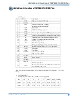
Definition & Function of TMPA8873-XXXX Pins
Definition & Function of TMPA8873-XXXX Pins
10.
CPU part
item
definition
description
1
DVD
high level output in DVD mode
2
NO USE
3
KEY
Control signal input; general
keyboard circuit auto identified
4
GND
MCU GND
5
REST
MCU reset when power on
6
X-TAC
7
X-TAC
Connect ports for crystal; 20PPM precision required
8
TEST
For MCU experimentation, connected to GND normal
9
5V
Power input for CCD amplitude restricted circuit
10
Vss
GND for CCD amplitude restricted circuit
54
GND
GND for surge circuit
55
5V
Power for surge circuit;
Duty cycle and Ripple voltage less than 10 mV;
56
AV SW
Multi-control level output 2 or 3 TV/AV mode
57
SDA
SDA input
58
SOL
SCL input
59
50/60HZ
Low level when 50HZ
High level when 60HZ
60
NO USE
61
MUTE
MUTE control
62
NO USE
63
RMT IN
RC unit signal input
64
Power
Power control; low level for initialization; related with
item ONTIME of Page F11
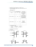
Note for control port output state: (in the output table below,”0”for low level, “1” for high
level)
Pin3 Description:
Voltage range for each button (middle value is suggested)
KEY
Off
P+
P-
V+
V-
MENU
TV/AV
POWER
Range
0V
≤
1.16V
≤
1.74V
≤
2.45V
≤
3.17V
≤
3.88V
≤
4.60V
≤
5V
Range
5V
0
≤
0.45V
≤
1.02V
≤
1.74V
≤
2.45V
≤
3.17V
≤
3.88V
≤
4.60V
Содержание TC1475
Страница 1: ...COLOR TELEVISION TC1475 TC2175 TF2139 TC1475 TC2175 TF2139 ...
Страница 6: ...TC1475 TC2175 TF2139 5 TMPA8873 XXXX Block Diagram TMPA8873 XXXX Block Diagram 3 1 ...
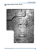
Страница 9: ...TC1475 TC2175 TF2139 8 Diagram Pictoric TC1475 TC2175 Diagram Pictoric 6 ...
Страница 10: ...TC1475 TC2175 TF2139 9 Diagram Pictoric TF2139 Diagram Pictoric 7 ...
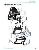
Страница 11: ...TC1475 TC2175 TF2139 10 Exploded View TC1475 TC2175 Exploded View 8 ...
Страница 12: ...TC1475 TC2175 TF2139 11 Exploded View TF2139 Exploded View 9 ...
Страница 28: ......


