
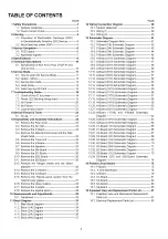


TABLE OF CONTENTS
1 Safety Precautions----------
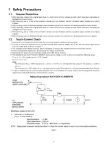
1.1. General Guidelines —
1.2. Touch-Current Check-
2 W arn in g ---------------------------
PAGE
------
3
------
3
------
3
------
4
2.1. Prevention of Electrostatic Discharge (ESD)
to Electrostatically Sensitive (ES) Devices---------- 4
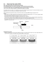
2.2. About lead free solder (PbF)-----------------------------5
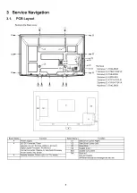
3 Service Navigation--------------------------------------------------- 6
3.1. PCB Layout----------------------------------------------------- 6
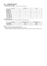
3.2. Applicable signals---------------------------------------------7
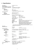
4 Specifications--------------------------------------------------------- 8
10
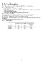
5 Technical Descriptions-----------------------------------
5.1. Specification of KEY for CI Plus, DTCP-IP and
One-to-One---------------------------------------------------- 10
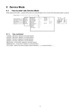
6 Service Mode---------------------------------------------------------- 11
6.1. How to enter into Service Mode------------------------- 11
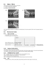
6.2. Option - Mirror------------------------------------------------- 13
6.3. Service tool mode--------------------------------------------13
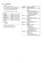
6.4. Hotel mode----------------------------------------------------- 14
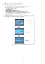
6.5. Data Copy by SD C ard ------------------------------------ 15
7 Troubleshooting Guide------------------------------------------- 18
7.1. Check of the IIC bus lines--------------------------------- 18
7.2. Power LED Blinking timing chart----------------------- 19
7.3. No Power------------------------------------------------------- 20
7.4. No Picture------------------------------------------------------ 21
7.5. Local screen failure----------------------------------------- 22
8 Service Fixture & Tools------------------------------------------ 23
8.1. SC jig ------------------------------------------------------------ 23
9 Disassembly and Assembly Instructions-----------------24
9.1. Remove the Rear cover----------------------------------24
9.2. Remove the AC inle t--------------------------------------24
9.3. Remove the P-Board-------------------------------------- 24
9.4. Remove the Side terminal cover and the Side
shield metal---------------------------------------------------- 24
9.5. Remove the Tuner u n it-----------------------------------25
9.6. Remove the A-Board--------------------------------------25
9.7. Remove the Speakers------------------------------------ 25
9.8. Remove the SM-Board----------------------------------- 25
9.9. Remove the SC-Board------------------------------------ 26
9.10. Remove the SS2-Board----------------------------------26
9.11. Remove the SS-Board------------------------------------ 26
9.12. Remove the Hanger metals and the Stand
brackets--------------------------------------------------------- 26
9.13. Remove the C1-Board------------------------------------ 27
9.14. Remove the C2-Board------------------------------------ 27
9.15. Remove the Plasma panel section from the
Cabinet assy (glass)---------------------------------------- 27
9.16. Remove the Glass holders----------------------------- 28
9.17. Remove the K-Board-------------------------------------- 28
9.18. Replace the plasma panel-------------------------------28
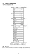
10.1. Adjustment----------------------------------------------------- 29
------------------------------------------------------
11.1. Main Block Diagram--------------------------------------- 33
11.2. Block (1/4) Diagram --------------------------------------- 34
11.3. Block (2/4) Diagram --------------------------------------- 35
11.4. Block (3/4) Diagram --------------------------------------- 36
11.5. Block (4/4) Diagram --------------------------------------- 37
12 Wiring Connection Diagram
12.1. Caution statement.------
12.2. Wiring ( 1 ) -------------------
12.3. Wiring (2) -------------------
13 Schematic Diagram
------------
PAGE
----
39
---- 39
---- 39
---- 40
----
41
---- 41
---- 42
---- 43
---- 44
---- 45
---- 46
---- 47
---- 48
---- 49
---- 50
---- 51
---- 52
---- 53
---- 54
---- 55
---- 56
---- 57
---- 58
---- 59
---- 60
---- 61
13.1. Schematic Diagram Note-------------------------
13.2. P-Board (1/4) Schematic Diagram------------
13.3. P-Board (2/4) Schematic Diagram------------
13.4. P-Board (3/4) Schematic Diagram------------
13.5. P-Board (4/4) Schematic Diagram------------
13.6. A-Board (1/19) Schematic Diagram-----------
13.7. A-Board (2/19) Schematic Diagram-----------
13.8. A-Board (3/19) Schematic Diagram-----------
13.9. A-Board (4/19) Schematic Diagram-----------
13.10. A-Board (5/19) Schematic Diagram-----------
13.11. A-Board (6/19) Schematic Diagram-----------
13.12. A-Board (7/19) Schematic Diagram-----------
13.13. A-Board (8/19) Schematic Diagram-----------
13.14. A-Board (9/19) Schematic Diagram-----------
13.15. A-Board (10/19) Schematic Diagram---------
13.16. A-Board (11/19) Schematic Diagram ---------
13.17. A-Board (12/19) Schematic Diagram---------
13.18. A-Board (13/19) Schematic Diagram---------
13.19. A-Board (14/19) Schematic Diagram---------
13.20. A-Board (15/19) Schematic Diagram---------
13.21. A-Board (16/19) Schematic Diagram---------
13.22. A-Board (17/19) and K-Board Schematic
Diagram -------------------------------------------------------- 62
13.23. A-Board (18/19) Schematic Diagram----------------- 63
13.24. A-Board (19/19) Schematic Diagram----------------- 64
13.25. C1-Board (1/2) Schematic D iagram ------------------ 65
13.26. C1-Board (2/2) Schematic D iagram ------------------ 66
13.27. C2-Board (1/2) Schematic D iagram ------------------ 67
13.28. C2-Board (2/2) Schematic D iagram ------------------ 68
13.29. SC-Board (1/4) Schematic Diagram------------------ 69
13.30. SC-Board (2/4) Schematic Diagram------------------ 70
13.31. SC-Board (3/4) Schematic Diagram-------------------71
13.32. SC-Board (4/4) Schematic Diagram------------------ 72
13.33. SS-Board (1/2) Schematic Diagram ------------------ 73
13.34. SS-Board (2/2) and SS2-Board Schematic
Diagram -------------------------------------------------------- 74
---------------------------------------------
14.1. P-Board---------------------------------------------------------75
14.2. K and SS2-Board-------------------------------------------78
14.3. A -B oard---------------------------------------------------------79
14.4. C1-Board-------------------------------------------------------- 81
14.5. C2-Board------------------------------------------------------- 82
14.6. SC-Board-------------------------------------------------------83
14.7. SS-Board ------------------------------------------------------ 85
15 Exploded View and Replacement Parts List------------- 87
15.1. Exploded View and Mechanical Replacement
Parts List------------------------------------------------------- 87
15.2. Electrical Replacement Parts L is t--------------------- 95
2
Содержание Viera TX-P42S20L
Страница 21: ...7 4 No Picture 21...
Страница 33: ...11 Block Diagram 11 1 Main Block Diagram 33...
Страница 34: ...11 2 Block 1 4 Diagram 34...
Страница 35: ...G 0 11 3 Block 2 4 Diagram I A I D IG IT A L S IG N A L P R O C E S S O R 35...
Страница 36: ...11 4 Block 3 4 Diagram P P O W E R S U P P LY 36...
Страница 37: ...11 5 Block 4 4 Diagram s c s c a n d r i v e s s s u s t a i n d r i v e 37...
Страница 38: ...38...
Страница 40: ...12 3 Wiring 2 40...
Страница 43: ...13 2 P Board 1 4 Schematic Diagram A B C D E A P BO ARD LSEP1287BE HB 1 4 F 1 2 3 4 42...
Страница 44: ...13 3 P Board 2 4 Schematic Diagram A P BO ARD LSEP1287BE HB 2 4 10 11 12 13 14 15 16 17 18 43...
Страница 45: ...13 4 P Board 3 4 Schematic Diagram A B C D E F 1 2 3 4 44 5...
Страница 46: ...13 5 P Board 4 4 Schematic Diagram 10 11 12 13 14 15 16 17 18 45...
Страница 47: ...13 6 A Board 1 19 Schematic Diagram A A A BO AR D 1 19 IIC B C D E F 1 2 3 4 9 46...
Страница 52: ...13 11 Board 6 19 Schematic Diagram A A BO AR D 6 19 STB MPU 46 47 48 49...
Страница 54: ...13 12 Board 7 19 Schematic Diagram A A BO AR D 7 1 9 HDMI 55 56 57 58 59 52...
Страница 57: ...69 70 71 72...
Страница 59: ...Peaks COM MON 78 79 80 81...
Страница 61: ...13 16 A Board 11 19 Schematic Diagram A A BO AR D 11 19 A V SW 91 92 93 94 95 96 97 98 99 56...
Страница 63: ...FE_Virtual_Module Peaks COMMON TO 3 19 Analog ASIC 104 105 106 107 108 57...
Страница 65: ...13 19 A Board 14 19 Schematic Diagram A A BO AR D 14 19 PD4H 118 119 120 121 122 123 124 125 126 59...
Страница 68: ...140 141 142 143 144 61...
Страница 71: ...63...
Страница 72: ...13 24 A Board 19 19 Schematic Diagram A A BO AR D 19 19 DVB T C D EM O D U LATO R 64...
Страница 75: ...13 27 C2 Board 1 2 Schematic Diagram A A C 2 BO AR D TN PA5095 1 2 ___ I TO A BOARD A32 B 67...
Страница 78: ...13 30 SC Board 2 4 Schematic Diagram 10 I 11 1 12 1 13 1 14 1 15 1 16 1 17 1 18 70...
Страница 79: ...13 31 SC Board 3 4 Schematic Diagram 19 1 20 1 21 1 22 1 23 1 24 1 25 1 26 1 27 71...
Страница 80: ...13 32 SC Board 4 4 Schematic Diagram 28 29 30 31 32 33 34 35 36 72...
Страница 81: ...13 33 SS Board 1 2 Schematic Diagram A B C D E A SS BO AR D TX N S S 11D E K 1 2 F 5 6 7 8 9 73...
Страница 86: ...P BOARD COMPONENT SIDE LSEP1287BEHB B G 6 5 4 3 2 1 E F H 77...
Страница 88: ...14 3 A Board 6 A BOARD FOIL SIDE A P42S20E A P42S20ES A P42S20L A PF42S20 A PR42S20 B G 5 4 3 2 1 E F H 79...
Страница 89: ...A BOARD COMPONENT SIDE A P42S20E A P42S20ES A P42S20L A PF42S20 A PR42S20 B G 6 5 4 3 2 1 E F H 80...
Страница 92: ...14 6 SC Board SC BOARD FOIL SIDE TXNSC11DEK B G 6 5 4 3 2 1 E F H 83...
Страница 93: ...SC BOARD COMPONENT SIDE TXNSC11DEK B G 6 5 4 3 2 1 E F H 84...
Страница 94: ...14 7 SS Board SS BOARD FOIL SIDE TXNSS11DEK B G 6 5 4 3 2 1 E F H 85...
Страница 95: ...SS BOARD COMPONENT SIDE TXNSS11DEK...
Страница 96: ......
Страница 98: ...15 1 2 Exploded View 2 88...
Страница 99: ...15 1 3 Packing 1 89...
Страница 100: ...15 1 4 Packing 2 90...


