5
TC-P42GT30A
2.2.
About lead free solder (PbF)
Note: Lead is listed as (Pb) in the periodic table of elements.
In the information below, Pb will refer to Lead solder, and PbF will refer to Lead Free Solder.
The Lead Free Solder used in our manufacturing process and discussed below is (Sn+Ag+Cu).
That is Tin (Sn), Silver (Ag) and Copper (Cu) although other types are available.
This model uses Pb Free solder in it's manufacture due to environmental conservation issues. For service and repair work, we'd
suggest the use of Pb free solder as well, although Pb solder may be used.
PCBs manufactured using lead free solder will have the PbF within a leaf Symbol
PbF
stamped on the back of PCB.
Caution
• Pb free solder has a higher melting point than stand
ard solder. Typically the melting point is 50 ~ 70
°
F (30~40
°
C) higher. Please
use a high temperature soldering iron and set it to 700 ± 20
°
F (370 ± 10
°
C).
• Pb free solder will tend to splash when heated too high (about 1100
°
F or 600
°
C).
If you must use Pb solder, please completely remove all of the Pb free solder on the pins or solder area before applying Pb sol-
der. If this is not practical, be sure to heat the Pb free solder until it melts, before applying Pb solder.
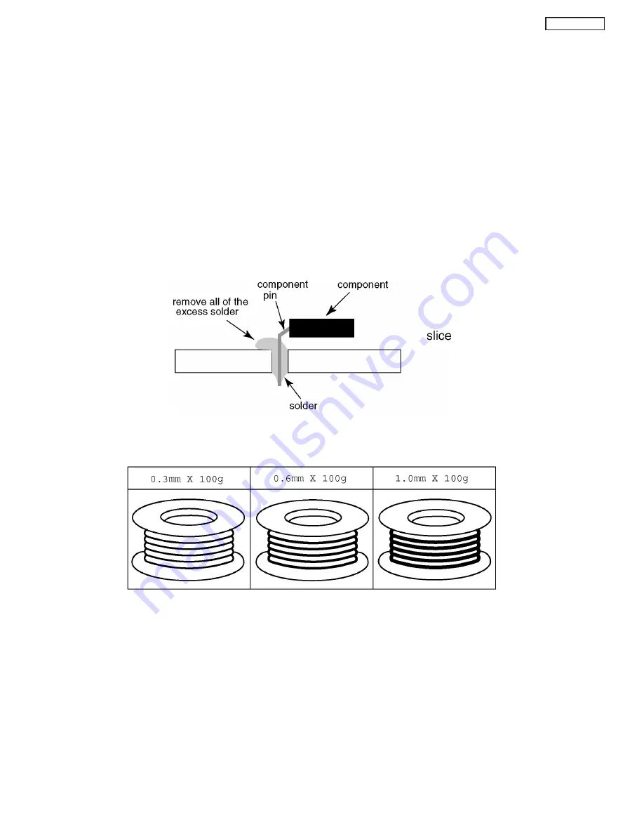
• After applying PbF solder to double layered boards, please check the component side for excess solder which may flow onto the
opposite side. (see figure below)
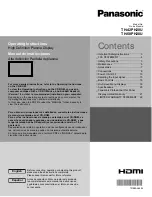
Suggested Pb free solder
There are several kinds of Pb free solder available for purchase
. This product uses Sn+Ag+Cu (tin, silver, copper) solder. How-
ever, Sn+Cu (tin, copper), Sn+Zn+Bi (tin, zinc, bismuth) solder can also be used.
Содержание TC-P42GT30A
Страница 19: ...19 TC P42GT30A 7 4 No Picture ...
Страница 33: ...33 TC P42GT30A ...
Страница 34: ...34 TC P42GT30A ...
Страница 41: ...41 TC P42GT30A 11 3 Wiring 2 11 4 Wiring 3 ...
Страница 42: ...42 TC P42GT30A 11 5 Wiring 4 11 6 Wiring 5 ...
Страница 43: ...43 TC P42GT30A Model No TH P42GT30A Schematic Diagram Note 12 Schematic Diagram 12 1 Schematic Diagram Note ...
Страница 45: ...45 TC P42GT30A 12 3 A Board Schematic Diagram 1 20 ...
Страница 67: ...67 TC P42GT30A 12 25 SS Board Schematic Diagram ...
Страница 74: ...74 TC P42GT30A 13 Printed Circuit Boards 13 1 P Board Foil side ...
Страница 75: ...75 TC P42GT30A 13 2 P Board Component side ...
Страница 76: ...76 TC P42GT30A 13 3 A Board Foil side ...
Страница 77: ...77 TC P42GT30A 13 4 A Board Component side ...
Страница 78: ...78 TC P42GT30A 13 5 K S and V Boards ...
Страница 79: ...79 TC P42GT30A 13 6 C1 Board 13 7 C2 Board ...
Страница 80: ...80 TC P42GT30A 13 8 SN Board Foil side ...
Страница 81: ...81 TC P42GT30A 13 9 SN Board Component side ...
Страница 82: ...82 TC P42GT30A 13 10 SS Board Foil side ...
Страница 83: ...83 TC P42GT30A 13 11 SS Board Component side ...
Страница 84: ...84 TC P42GT30A 13 12 SS2 Board ...
Страница 87: ...87 TC P42GT30A 14 2 2 Packing and Accessories Exploded View Stand mounting kit Positionig hole 3 ...
Страница 112: ...Panasonic do Brasil Limitada DIVISÃO CS SETOR DE APOIO TÉCNICO Rod Presidente Dutra Km 155 São José dos Campos SP ...


