background image

Item

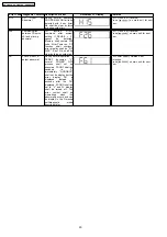
FL Display

Key Operation

Mode Name

Description

Front Key

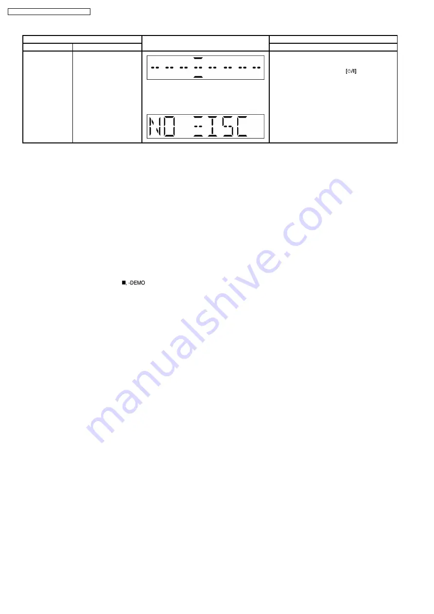
Cold Start

To activate cold start
ipon next AC power up.

Note:

This test do not work when selector is in

Tuner.

The [NO DISC] display will appear after 3 sec.

In doctor mode:
 1. 

Press [SLEEP] button on remote control.

To exit Doctor Mode, press

button on

main unit or remote control.

8.2.3. CD to Tape Recording Inspection

Purpose : To check the recording function from CD to Tape.
Below is the procedures for this mode:-
Step 1: Enter into Doctor mode (For more information refer to section 8.2 on key operation to enter into this mode).
Step 2: Insert Test disc (CDT-018). Note: Ensure TOC is completed before next step.
Step 3: Press [4] button on remote control. (It enter into CD to Tape Test mode. The volume is set to [50dB], Bass & Treble is set
to 0dB & EQ is switch off).

Note :

When in this mode, the following processes is perform :

a) Deck will rewind to the start point (point at the start of recording) & stop.
b) Recording begins (at constant analogue recording speed) for 3 seconds & stop.


·


However, “Error” would be display if there is no tracks to access to, no tape inserted, no test CD inserted or when the tape
erasure prevention tab for FWD side is not suitable for recording.


·


To exit from this mode, press [

] button on main uint.

8.2.4. Tape Recording and Playing

Purpose : To check the tape operating function. (Playability & record function)
Note:
Below is the procedures for this mode:-
Step 1: Enter into Doctor mode (For more information refer to section 8.2 on key operation to enter into this mode).
Step 2: Press [5] button on remote control. (During this mode, tape function is set to automatically, volume is set to [50dB], Bass
& Treble is set to 0dB & EQ is switch off).
Step 3: The tape played for 3 seconds after which it stop & eject. (Cassette door opens automatically)

Note :

When in CD to Tape Recording Test mode, the following process is perform :

a) If the erasure prevention tab for FWD side the tape is broken, it is judged as an error and the recording operation does not start.
b) If tape stops by detecting a tape end while recording, it becomes an error.
c) If STOP key is pressed while recording or playing, the operation shall be terminated by stopping TAPE. In this case, the doctor
mode is not released.
d) DMT is output with the same timing as usual.

16

SA-PM45E / SA-PM45EG / SA-PM45EE

Содержание SA-PM45E

Страница 1: ...annel 2007 Matsushita Electric Industrial Co Ltd All rights reserved Unauthorized copying and distribution is a violation of law SA PM45E SA PM45EG SA PM45EE Colour K Black Type Heads Record playback Solid permalloy head Erasure Double gap ferrite head Motor DC servo motor Recording system AC bias 100 kHz Erase system AC erase 100 kHz Tape speed 4 8 cm s Overall frequency response 3 6 dB at DECK O...

Страница 2: ... V 50 Hz Power consumption 63 W Dimensions W x H x D 164 mm x 227 mm x 314 mm Mass 3 4 kg Operating temperature range 5 to 35 C Operating humidity range 5 to 90 RH no condensation Power consumption in standby mode 0 6 W approx Notes 1 Specifications are subject to change without notices Mass and dimensions are approximate 2 Total harmonic distortion is measured by the digital spectrum analyzer n S...

Страница 3: ...B MODULE 61 15 4 MAIN 2 2 PANEL 62 16 Notes of Schematic Diagram 63 17 Schematic Diagram 65 17 1 CD SERVO CIRCUIT 65 17 2 MAIN CIRCUIT 66 17 3 PANEL CIRCUIT 70 17 4 TRANSFORMER CIRCUIT DECK MECHANISM CIRCUIT TAPE EJECT CIRCUIT 71 17 5 DECK CIRCUIT 72 17 6 USB CIRCUIT 73 18 Printed Circuit Board Diagrams 75 18 1 CD SERVO P C B DECK P C B DECK MECHANISM P C B and TAPE EJECT P C B 75 18 2 MAIN P C B ...

Страница 4: ...e a return path to the chassis the reading must be 1 1 2 LEAKAGE CURRENT HOT CHECK See Figure 1 1 Plug the AC cord directly into the AC outlet Do not use an isolation transformer for this check 2 Connect a 1 5kΩ 10 watts resistor in parallel with a 0 15µF capacitors between each exposed metallic part on the set and a good earth ground such as a water pipe as shown in Figure 1 3 Use an AC voltmeter...

Страница 5: ...cedure outlines below 1 Turn off the power 2 Determine the cause of the problem and correct it 3 Turn on the power once again after one minute Note When the protection circuitry functions the unit will not operate unless the power is first turned off and then on again 1 4 Safety Part Information Safety Parts List There are special components used in this equipment which are important for safety Th...

Страница 6: ...se only a grounded tip soldering iron to solder or unsolder ES devices 4 Use only an anti static solder removal device Some solder removal devices not classified as anti static ESD protected can generate electrical charge to damage ES devices 5 Do not use freon propelled chemicals These can generate electrical charges sufficient to damage ES devices 6 Do not remove a replacement ES device from its...

Страница 7: ...ine Laserdiode Im eingeschalteten Zustand wird unsichtbare Laserstrahlung von der Lasereinheit abgestrahlt Wellenlänge 780nm Maximale Strahlungsleistung der Lasereinheit 100 µW VDE Die Strahlung an der Lasereinheit ist ungefährlich wenn folgende Punkte beachtet werden 1 Die Lasereinheit nicht zerlegen da die Strahlung an der freigelegten Laserdiode gefährlich ist 2 Den werkseitig justierten Einste...

Страница 8: ...in as short time as possible Fig 4 1 4 Do not turn the variable resistor laser power adjustment It has already been adjusted Grounding for electrostatic breakdown prevention 1 Work table grounding Fig 4 2 Use the anti static wrist strap to discharge the static electricity from your body 2 Work table grounding Fig 4 2 Put a conductive material sheet or steel sheet on the area where the traverse dec...

Страница 9: ...he lead free solder has to be used when repairing the equipment for which the lead free solder is used Definition The letter of PbF is printed on the PCB using the lead free solder To put lead free solder it should be well molten and mixed with the original lead free solder Remove the remaining lead free solder on the PCB cleanly for soldering of the new IC Since the melting point of the lead free...

Страница 10: ...6 Accessories Note Refer to Packing Materials Accessories Parts List Section 22 for the part number Remote Control AC Cord FM Antenna AM Loop Antenna 10 SA PM45E SA PM45EG SA PM45EE ...

Страница 11: ...7 Operation Procedures 7 1 Main Unit Key Buttons Operation 11 SA PM45E SA PM45EG SA PM45EE ...

Страница 12: ...7 2 Remote Control Key Buttons Operation 7 3 Disc Information 12 SA PM45E SA PM45EG SA PM45EE ...

Страница 13: ...lume 50 setting check Refer to section 8 2 service mode Table 1 2 for more information 8 Volume 29 setting check Refer to section 8 2 service mode Table 1 2 for more information 9 Volume 0 setting check Refer to section 8 2 service mode Table 1 2 for more information 1 1 CD Loading Test Mode Refer to section 8 2 service mode Table 1 2 for more information 1 2 CD Traverse Unit Test Mode Refer to se...

Страница 14: ...ol 8 2 2 Service Mode Table 2 Item FL Display Key Operation Mode Name Description Front Key FL Display Test To check the FL segments display All segments will light up In doctor mode 1 Press DIMMER button on remote control To cancel press 0 button on remote control To exit Doctor Mode press button on main unit or remote control CD to Tape Recording Test Mode To Inspect the recording process from C...

Страница 15: ...main unit or remote control CD Traverse Unit Test Mode To check for the traverse unit operation In this made the first lost track is access read TOC It fails when TOC is not completed by IDS or the traverse is out of focus In doctor Mode 1 Press 1 2 button on remote control To cancel press 0 button on remote control To exit Doctor Mode press button on main unit or remote control CD Combination Tes...

Страница 16: ...lay if there is no tracks to access to no tape inserted no test CD inserted or when the tape erasure prevention tab for FWD side is not suitable for recording To exit from this mode press button on main uint 8 2 4 Tape Recording and Playing Purpose To check the tape operating function Playability record function Note Below is the procedures for this mode Step 1 Enter into Doctor mode For more info...

Страница 17: ...ction 8 2 on key operation to enter into this mode Step 2 When 1 4 key are pressed at the doctor mode the following shall be displayed for 3 secs The result shall correspond to the condition met as shown in the table below 8 2 6 TPS Inspection Purpose Tape for TPS is put into Deck TPS inspection starts with one key operation This mode shall run a test program to check 17 SA PM45E SA PM45EG SA PM45...

Страница 18: ...icro processor will start checking for the existence of cassette in deck mechanism unit If it does not contain any cassette it shall end the test and displays ERROR If the cassette is detected test shall start by playing the DECK in reverse direction for 1 sec and perform REV TPS If TPS signal is OK the Deck shall be ejected Below is information on the TPS under 3 examples 1 If ERROR Flag is set E...

Страница 19: ...abnormality item code in the following sequence TEST H 0 1 TEST H 0 2 TEST H 0 3 7 To clear all the abnormalities in the memory press the n Key for more than 5 Sec while the self diagnostic mode is stopped At this time all the abnormalities item in the memory is cleared and is displayed on the LCD C L E A R display for 1 Sec then TEST is displayed 8 To cancel the self diagnostic mode press the Key...

Страница 20: ...splay shall be NO DISC Error No shall be clear by force or cold start For CD unit For Traverse Press on main unit for next error F61 POWER AMP IC output abnormal During normal operation if DCDET becomes L normal POWER OFF process shall not be executed PCONT shall be switched to L immediately GOODBYE shall not be display but the error display F61 is displayed instead 2 seconds after the F61 display...

Страница 21: ...replacement are required Warning This product uses a laser diode Refer to Precaution of Laser Diode ACHTUNG Die Lasereinheit nicht zerlegen Die Lasereinheit darf nur gegen eine vom Hertsteller spezifizierte Einheit ausgetauscht werden Below is the list of disassembly sections Disassembly of Side Panel L R Disassembly of Top Cabinet Unit Disassembly of Deck Mechanism Tape Eject P C B Disassembly of...

Страница 22: ... following chart is the procedure for disassembling the casing and inside parts for internal inspection when carrying out the servicing To assemble the unit reverse the steps shown in the chart below 22 SA PM45E SA PM45EG SA PM45EE ...

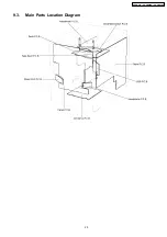
Страница 23: ...9 3 Main Parts Location Diagram 23 SA PM45E SA PM45EG SA PM45EE ...

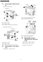
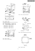
Страница 24: ...he Side Panel L as arrow shown 9 5 Disassembly of Top Cabinet Unit Follow the Step 1 Step 6 of Item 9 4 Step 1 Lift up the top cabinet as arrow shown Note Be careful of the catches area Step 2 Disconnect FFC cable CN804 Step 3 Remove Top Cabinet Unit 9 6 Disassembly of Deck Mechanism and Tape Eject P C B Follow the Step 1 Step 6 of Item 9 4 Follow the Step 1 Step 3 of Item 9 5 Diasssembly of Tape ...

Страница 25: ... Lid Follow the Step 1 Step 6 of Item 9 4 Follow the Step 1 Step 3 of Item 9 5 When opening the disc tray automatically Using Power Supply Step 1 Connect the AC power cord Step 2 Press the POWER button to power up the main unit Step 3 Press the OPEN CLOSE button the disc tray will be open automatically Step 4 Release the 2 claws Step 5 Remove the CD Lid as arrow shown Step 6 Press the OPEN CLOSE b...

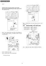
Страница 26: ... the direction of arrow The disc tray will be open Step 2 Release the 2 claws Step 3 Remove the CD Lid as arrow shown To close the CD tray Step 4 Repeat Step 1 but rotate the gear tools in anti clockwiser 9 8 Disassembly of Front Panel Follow the Step 1 Step 6 of Item 9 4 Follow the Step 1 Step 3 of Item 9 5 Follow the Step 1 Step 6 of Item 9 7 Step 1 Detach wire cable CN802 CN900B and CN901B 26 S...

Страница 27: ...B Follow the Step 1 Step 6 of Item 9 4 Follow the Step 1 Step 3 of Item 9 5 Follow the Step 1 Step 6 of Item 9 7 Follow the Step 1 Step 3 of Item 9 8 Step 1 Remove 2 screws Step 2 Remove the USB Ornament Step 3 Remove 2 screws and USB Unit Step 4 Remove USB bottom case as arrow shown Step 5 Unsolder 4 points 27 SA PM45E SA PM45EG SA PM45EE ...

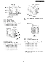
Страница 28: ... 9 8 Disassembly of Headphone P C B Step 1 Remove 2 screws Step 2 Remove the USB Ornament Step 3 Remove 1 screw Step 4 Release the clutch Step 5 Remove the Headphone P C B Disassembly of Music Port P C B Step 6 Remove 2 screws Step 7 Remove the Phone Ornament Step 8 Remove 1 screw Step 9 Release the clutch Step 10 Remove the Music Port P C B Disassembly of Panel P C B Step 11 Remove the Volume Kno...

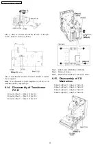
Страница 29: ...tep 1 Step 6 of Item 9 7 Follow the Step 1 Step 3 of Item 9 8 Follow the Step 1 Step 2 of Item 9 11 Step 1 Detach cables CN807 CN505B and CD Open Switch Step 2 Remove 1 screw Step 3 Remove Main P C B as arrow shown 9 13 Replacement of the Power IC Follow the Step 1 Step 6 of Item 9 4 Follow the Step 1 Step 3 of Item 9 5 Follow the Step 1 Step 6 of Item 9 7 Follow the Step 1 Step 3 of Item 9 8 Foll...

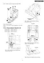
Страница 30: ...y of Transformer P C B Follow the Step 1 Step 6 of Item 9 4 Follow the Step 1 Step 3 of Item 9 5 Follow the Step 1 Step 2 of Item 9 11 Step 1 Detach cable CN900B and CN505B Step 2 Remove 4 screws Step 3 Remove Transformer P C B as arrow shown 9 15 Disassembly of CD Mechanism Follow the Step 1 Step 6 of Item 9 4 Follow the Step 1 Step 3 of Item 9 5 Follow the Step 1 Step 6 of Item 9 7 Follow the St...

Страница 31: ... Step 6 of Item 9 4 Follow the Step 1 Step 3 of Item 9 5 Follow the Step 1 step 6 of Item 9 6 Step 1 Using screwdriver to remove Damper gear as arrow shown in order Step 2 Remove the Cassette Open Spring as arrow shown in order Step 3 Pull the sides Cassette holders to the direction of the arrows shown Step 4 Remove the Cassette Lid as arrows shown 31 SA PM45E SA PM45EG SA PM45EE ...

Страница 32: ...ssembly of the Traverse Unit Follow the Step 1 Step 6 of Item 9 4 Follow the Step 1 Step 3 of Item 9 5 Follow the Step 1 Step 6 of Item 9 7 Follow the Step 1 Step 3 of Item 9 8 Follow the Step 1 Step 3 of Item 9 15 Disassembly of gears drive 32 SA PM45E SA PM45EG SA PM45EE ...

Страница 33: ...33 SA PM45E SA PM45EG SA PM45EE ...

Страница 34: ...9 17 2 Disassembly of CD Servo P C B Follow the Step 1 Step 6 of Item 9 4 Follow the Step 1 Step 3 of Item 9 5 Follow the Step 1 Step 6 of Item 9 7 34 SA PM45E SA PM45EG SA PM45EE ...

Страница 35: ... 9 17 3 Disassembly of Traverse Gear A and Traverse Gear B Follow the Step 1 Step 6 of Item 9 4 Follow the Step 1 Step 3 of Item 9 5 Follow the Step 1 Step 6 of Item 9 7 Follow the Step 1 Step 3 of Item 9 8 Follow the Step 1 Step 3 of Item 9 15 Follow the Step 1 Step 4 of Item 9 17 1 35 SA PM45E SA PM45EG SA PM45EE ...

Страница 36: ...ow the Step 1 Step 3 of Item 9 5 Follow the Step 1 Step 6 of Item 9 6 9 18 2 Disassembly of Motor Capstan Belt A Capstan Belt B and Winding Belt Deck Mechanism Unit Follow the Step 1 Step 6 of Item 9 4 Follow the Step 1 Step 3 of Item 9 5 Follow the Step 1 Step 6 of Item 9 6 Follow the Step 1 Step 4 of Item 9 18 1 36 SA PM45E SA PM45EG SA PM45EE ...

Страница 37: ...37 SA PM45E SA PM45EG SA PM45EE ...

Страница 38: ... of Item 9 18 1 9 19 Handling of cassette tape jam Follow the Step 4 Step 6 of Item 9 4 Step 1 If the cassette tape cannot eject due to twinning around capstan or pinch roller during play or record rotate the Winding Arm as arrow shown to remove twined tape Step 2 Push the lever as arrow shown to open the cassette lid and remove the cassette tape 38 SA PM45E SA PM45EG SA PM45EE ...

Страница 39: ...10 Service Positions Note For description of the disassembly procedures see the Section 9 10 1 Check and Repair of Deck Deck Mechanism Tape Eject P C B 39 SA PM45E SA PM45EG SA PM45EE ...

Страница 40: ...10 2 Check and Repair of Panel Headphone Music Port P C B 40 SA PM45E SA PM45EG SA PM45EE ...

Страница 41: ...10 3 Check and Repair of Transformer P C B 41 SA PM45E SA PM45EG SA PM45EE ...

Страница 42: ...10 4 Check and Repair of Main P C B 42 SA PM45E SA PM45EG SA PM45EE ...

Страница 43: ...10 5 Check and Repair of CD Servo P C B Note Connect AC power cord and switch on the set Eject tray loading load in CD and switch off the set Proceed with checking 43 SA PM45E SA PM45EG SA PM45EE ...

Страница 44: ...10 6 Check and Repair of USB P C B Side A 44 SA PM45E SA PM45EG SA PM45EE ...

Страница 45: ...10 7 Check and Repair of USB P C B Side B 45 SA PM45E SA PM45EG SA PM45EE ...

Страница 46: ...ng at STOP mode ON approx 200msec e REV REW Supply the plunger power in a flash at REV PLAY mode ON approx 50msec f STOP Supply the plunger power in a flash at FF mode ON approx 50msec Repeat the operation FWD PLAY Note Other operation may start if a timing of supplying the plunger power is missed 11 1 1 Connection Status between Mechanism and Power Supply Motor Plunger 11 1 2 Operative Parts of M...

Страница 47: ...Fig 7 47 SA PM45E SA PM45EG SA PM45EE ...

Страница 48: ...emove 4 screws from the mechanism unit to disassemble under 9 Assembling and Disassembling 3 Connect the headphone jack output jig Fig 8 to headphone jack Fig 8 Fig 9 12 1 4 Tape Speed Adjustment Normal speed adjustment only during forward playback Product reference value 3 000 90Hz 1 Connect a frequency indicator Fig 12 2 Playback the middle portion of the test tape QZZCWAT 3 Adjust the motor scr...

Страница 49: ...t pressing the buttons till the recording pause mode is activated 5 Check that the output level is within the standard range Standard Range 16 3mV Fig 12 12 1 6 Bias Frequency Check 1 Connect a digital frequency counter Fig 13 2 Set the function to TAPE position 3 Insert a normal blank cassette tape QZZCRA and press REC mode on main unit 4 Check that the output frequency is within the standard ran...

Страница 50: ...1 6 1 6 0 0 1 9 1 9 0 1 7 1 7 STANDBY 0 0 0 0 0 0 0 0 0 0 0 0 0 0 0 0 0 0 0 0 Ref No MODE 41 42 43 44 45 46 47 48 49 50 51 52 53 54 55 56 57 58 59 60 CD PLAY 0 2 2 4 1 7 1 9 1 0 3 2 1 2 0 1 2 1 6 1 6 0 9 1 4 1 5 1 5 0 3 2 0 0 STANDBY 0 0 0 0 0 0 0 0 0 0 0 0 0 0 0 0 0 0 0 0 Ref No MODE 61 62 63 64 65 66 67 68 69 70 71 72 73 74 75 76 77 78 79 80 CD PLAY 3 2 0 0 0 0 0 3 3 3 2 9 0 3 2 0 1 6 0 1 6 3 2 ...

Страница 51: ...0 0 0 0 0 0 0 0 0 1 5 1 5 0 1 5 1 6 3 2 1 8 3 1 0 Ref No MODE 21 22 23 24 25 26 27 28 29 30 31 32 33 34 35 36 37 38 39 40 CD PLAY 0 0 0 0 3 2 2 1 3 1 3 0 2 3 3 2 8 3 0 3 3 2 1 8 0 0 0 STANDBY 0 0 0 0 3 2 2 1 3 1 3 0 2 5 0 0 0 0 0 0 0 0 0 0 Ref No MODE 41 42 43 44 45 46 47 48 49 50 51 52 53 54 55 56 57 58 59 60 CD PLAY 0 0 0 0 3 0 1 5 1 5 0 0 3 3 3 0 0 1 2 1 2 1 2 1 2 1 2 STANDBY 0 0 0 0 0 0 1 5 1 ...

Страница 52: ... 0 3 0 3 0 1 0 0 0 0 1 0 0 0 0 0 0 0 1 0 0 0 0 1 0 3 STANDBY 0 0 3 0 3 0 1 0 0 0 0 1 0 0 0 0 0 0 0 1 0 0 0 0 1 0 3 Ref No MODE 21 22 CD PLAY 0 3 0 STANDBY 0 3 0 Ref No MODE E C B E C B E C B E C B E C B CD PLAY 0 0 0 7 0 0 0 7 9 8 9 7 0 0 0 0 0 0 0 STANDBY 0 0 0 0 0 0 0 3 0 0 0 0 0 0 0 0 Ref No MODE E C B E C B E C B E C B E C B CD PLAY 0 0 0 0 0 0 0 0 0 3 3 0 5 3 1 7 9 1 STANDBY 0 0 0 0 0 0 0 0 0...

Страница 53: ...4 35 36 37 38 39 40 CD PLAY 3 3 3 3 3 3 1 4 1 4 1 3 1 3 1 3 1 3 1 3 1 3 1 3 1 3 1 3 1 3 1 3 1 3 3 3 1 4 0 STANDBY 0 0 0 0 0 0 0 0 0 0 0 0 1 0 0 0 0 0 0 0 0 Ref No MODE 41 42 43 44 45 46 47 48 49 50 51 52 53 54 55 56 57 58 59 60 CD PLAY 1 4 1 2 1 8 0 1 4 3 2 3 2 0 1 3 2 0 0 1 2 0 1 0 1 4 3 1 3 1 3 1 0 1 3 STANDBY 0 0 0 0 0 0 0 0 0 0 0 0 0 0 0 0 0 0 0 0 Ref No MODE 61 62 63 64 CD PLAY 0 1 8 1 4 3 2 ...

Страница 54: ...50msec div CN901B PIN 8 CD PLAY 3 32Vp p 50msec div IC803 PIN 4 CD PLAY 3 28Vp p 25usec div IC803 PIN 6 CD PLAY 3 32Vp p 50usec div CN802 PIN 15 CD PLAY 3 44Vp p 5msec div IC803 PIN 12 CD PLAY 3 00Vp p 50nsec div IC803 PIN 13 CD PLAY 1 50Vp p 50nsec div IC803 PIN 16 CD PLAY 3 20Vp p 25usec div IC803 PIN 33 CD PLAY 3 52Vp p 5msec div IC803 PIN 74 CD PLAY 792mVp p 500usec div IC7001 PIN 25 CD PLAY 1...

Страница 55: ...IC7001 PIN 68 CD PLAY 3 44Vp p 10msec div IC7001 PIN 80 CD PLAY 4 24Vp p 25nsec div 55 SA PM45E SA PM45EG SA PM45EE ...

Страница 56: ...56 SA PM45E SA PM45EG SA PM45EE ...

Страница 57: ...DECK P C B SOLDER SIDE 1 2 3 4 5 1 9 19 1 18 2 MOTOR 1 2 1 19 2 18 1 12 2 22 1 21 1 21 2 22 19 1 18 2 PbF B MAIN P C B SOLDER SIDE CN802 Ref no 5 CN901B CN803 JK501 CN804 CN807 1 2 SENSOR VOLUME 1 4 1 2 3 1 5 18 2 19 1 PbF C PANEL P C B SOLDER SIDE VR900 WH900 Z901 WH301A WH401A CN901A 4 1 PbF D HEADPHONE P C B SOLDER SIDE JK900 WH504 3 2 1 PbF E MUSIC PORT P C B SOLDER SIDE JK303 WH301B JW308A 1 ...

Страница 58: ...SA PM45E SA PM45EG SA PM45EE 58 ...

Страница 59: ... 2 12 2 4 8 0 642 0 0 6482 52176 2 0 2 84 28 28 8 64 8 45 1614 52 0 1614 126 2 72 2 5 481 2 1 75 1 64 0 1 6 126 2 72 2 161 6 614 5 10 7 614 5 4 6 A 8 2 84 84 84 8 8 3 59 6 0 5 481 241 5514 6 5 0 241 5514 6 6 4 108 46 4 176 8 1 24 8 1 4 10 06 56 4 6 6 0 0 0 0 1764 0 0 0 0 0 0 0 0 0 0 0 0 5 2 5 481 126 2 72 70 6 1 4 4 5 6 59 6 SA PM45E SA PM45EG SA PM45EE 59 ...

Страница 60: ...176 2 4 59 59 6 1 014 41 59 8 4 4 176 4 0 6 4 6 4 4 2 4 22 4 6 10 76 2 4 0 2 4 0 2 4 3 2 4176 4 4 176 4 4 0 4 2 76 3 3 3 3 6 2411 8 59 6 4 5 4 2 4 2 4 5 1 5 5 4 0A 3 3 76 0 59 6 3 76 0 59 6 59 6 76 0 106 5 59 6 3 59 6 5 59 6 1614 5722 0 0 0 0 0 0 0 0 0 0 0 0 0 0 0 0 0 0 0 0 0 0 0 0 6 6 3 5 5 8 8 A 8 4 7 614 5 5 8 3 2 106 59 6 3 59 6 57 A 8 61 52 3 82 81 6 4 7 614 6 2 6 59 2 0 0 0 0 0 0 0 0 4 5 2 0...

Страница 61: ...0 0 0 0 0 0 0 0 0 A56 6 A12 0A59 15 A 4 56A59 12 0A 75 A456 1 6 44 8 44 75 A5 75 A4 3 75 A5 12 0 59 0 0 A 6 A 456 A 52A 6 52A 52A 6 670 4A 6 670 4A4 6 52A 6 2 106A 76 2 106A 2 106A 0 0 81 A 1 81 A 1 4 6 A5641 A 6 1 A5 A 1 A5 A 6 56 0 564 3 56 A56 6 A 0456 A 6 A4 3 A A0456 A 8 8 6 0 0456 176 8 8 855 8 84 0 0 0 0 0 0 0 0 0 0 0 0 0 0 0 0 0 0 0 0 0 0 0 0 2 2 2 2 0 0 0 2 75 75 8 44 6 44 1 8 8 8 0 5 75 ...

Страница 62: ...3 59 6 76 3 76 0 59 6 4 4 76 176A4 176A 56 0A 0A4 176A4 176A 6 4 6 4 0 0 0 0 0 0 0 0 8 0 0 0 0 0 0 0 0 0 0 8 2 8 A 8 8 8 8 57 A 8 5 5 8 A 8 8 8 75 A 8 6 0 8 8 8 6 0 3 8 59 6 61 1 4 61 5 481 1 4 0 0 8 8R 8 8 8R 52A 6 52A 670 4A 6 670 4A4 6 5 5 8 2 106A 84 8 0 2 0 0 0 0 0 0 0 0 0 0 0 0 0 0 5 0 0 5 0 5 0 0 5 0 0 5 0 0 5 0 0 7 5 0 0 6 2 4 14 5 0 0 75 5 0 0 6 2 2 5 0 0 5 2 0 2 0 1 4 4 4 81 7 1 59 75 21...

Страница 63: ... mark have special characteristics important for safety Furthermore special parts which have purposes of fire retardant resistors high quality sound capacitors low noise resistors etc are used When replacing any of components be sure to use only manufacturer s specified parts shown in the parts list Capacitor values are in microfarad µF unless specified otherwise F Farad pF Pico Farad Resistance v...

Страница 64: ...64 SA PM45E SA PM45EG SA PM45EE ...

Страница 65: ...36 100 R7335 1k R7332 22k R7331 3 3k R7323 330 R7325 1k R7329 C7352 0 018 1k R7339 C7338 0 056 19 18 17 20 15 16 14 12 9 11 10 13 22 23 30 21 28 27 24 25 26 2 1 6 7 29 8 3 4 5 IC7002 BA5948FPE2 4 CH DRIVE IC MLD 7 5V MCLK MDATA RST STAT BLKCK PGND 3 3V ST_IN TX LD SW DGND ST_CLK AGND AGND DGND ST_REQ RESET_SW LCH OUT RCH OUT LOADING A9 A11 TRP TRVP BA1 A0 A2 A4 A6 A8 A7 A5 A3 A1 A10 NWE BA0 PC NRA...

Страница 66: ...C101JA0027 L807 G0C101JA0027 4 3 7 5 6 1 2 9 10 8 Z401 ENG07823QF TUNER PACK R209 18K SDA DET STEREO A9V TUNED CL CD_LCH CD_RCH 6 8K R204 R403 2 7K 2 7K R203 PB_RCH 6 8K R404 C202 220P 220P C403 C203 220P 15K R206 R406 15K C405 220P C401 220P C201 220P 5 6K R201 MP_RCH MP_LCH 8 2K R211 R207 4 7K 4 7K R205 5 6K R401 TUNER_LCH TUNER_LCH TUNER_RCH TUNER_RCH 8 2K R411 C210 220P 220P C410 5 6K R202 5 6...

Страница 67: ...2 C374 50V10 56K R456 C351 470P 470P C373 11 4 3 6 7 8 9 5 1 2 10 12 IC300 AN17831A POWER AMP IC 220 R322 16V10 C320 R324 1K 560P C323 D3 3V LB320 C322 16V47 1000P C324 470P C321 1K R325 RMT FL_CS FL_CLK FL_DATA VOL_JOG1 DET D3 3V HP_SW 220 R323 7 5 6 1 2 4 3 10 12 14 15 16 13 11 8 9 IC301 C1AB00002751 RDS IC IC301 D3 3V LB321 LB320 LB321 J0JBC0000015 R321 2 2K 16V47 C325 C326 47P 47P C327 X320 X3...

Страница 68: ...T_SW R803 10K 100K R928 100 R809 100 R808 100 R807 100 R812 R810 100 R811 100 L803 L802 L803 J0JKB0000020 L802 1000P C812 1000P C810 STAT CD_RST USB_SDA LOADING CD_OPEN_SW USB_RST CD_MLD CD_MDATA BLKCK CD_MCLK D3 3V CD_LCH CD_RCH C216 1000P C416 1000P USB5V D3 3V VERR USB_IRQ DGND USB5V USB_SCL STIN DGND TERR STCLK DGND DGND MMOD DGND D3 3V CD_RST CD_CLK STREQ CD_DATA CD_STAT CD_MLD USB_RST USB_SD...

Страница 69: ...EGULATOR IC IC102 GND 2 4 1 3 5 IC101 C0DAZYY00006 CD 7 5V REGULATOR IC IC101 CD_7 5V SUB B_GND MOTOR_9V GND VCC_16V VCC_16V GND SUB B_11V HALT PCONT_1 GND2 GND1 SYS6V V02 CTL V01 VCC GND V02 CTL V01 VCC GND USB5V A9V CD_7 5V D3 3V VCC D9V SCHEMATIC DIAGRAM 5 TO MAIN SECTION 3 4 TO MAIN SECTION 2 4 MAIN CIRCUIT B SIGNAL LINE SA PM45E EE EG MAIN CIRCUIT 3 4 4 4 1 4 2 4 TO TRANSFORMER CIRCUIT CN505B...

Страница 70: ... 3V47 VREF D906 B3AAA0000489 STANDBY LED 100P C921 C920 100P 10K R822 R924 100K R925 100K VOL_JOG2 KEY1 S912 R914 3 3K S905 4 7K R906 4 7K R905 R912 1 5K S909 2 2K R913 S911 S910 GND2 L905 G0C101JA0027 2 3 1 5 4 WH900 1 5K R907 S901 S902 3 3K R904 S904 2 2K R903 S903 USB MPORT REC FF REW OPEN CLOSE TUNER BASS TREBLE TAPE CD GND2 WH401A WH301B WH504 GND FL1 FL2 SYS6V POWER STOP VP 21 SEG9 22 SEG8 3...

Страница 71: ...SFORMER DECK MECHANISM TAPE EJECT CIRCUIT TRANSFORMER CIRCUIT F2 F1 Z600 ERZV10V511CS JK600 AC IN 230V 50Hz 4 3 1 2 L600 G0B371HA0005 10 8 9 7 16 15 17 12 11 14 13 4 5 2 1 3 6 T601 G4CYAYY00139 POWER TRANSFORMER FP601 5A 3 4 1 2 RL600 K6B1AEA00015 7 6 3 2 9 T600 G4CYAYY00137 SUB TRANSFORMER 50V0 1u C613 50V0 1u C614 ECQE2104KF3 D617 D619 D618 F1 250V T630mA VP 2 3 1 5 4 CN900B SYS6V FL1 FL2 GND2 G...

Страница 72: ...204 10K C1222 0 01 C1208 16V10 R1305 10K C1305 16V33 C1308 16V22 R1307 22 R1308 22 C1109 50V3 3 C1210 6800P R1206 100K R1207 1K R1209 1K R1313 10K C1310 50V0 1 R1309 470 R1110 33K R1210 33K R1107 1K R1109 1K R1205 2 2K C1110 6800P R1106 100K R1105 2 2K C1209 50V3 3 R1371 22K AN6 AN7 VREF VREF PLVCC GND2 PHOTO VREF VREF PHOTO PLVCC RECH PHOTO VREF 9VGND RECH 9V DMT PHOTO REC_RIN TAPE_EJECT REC_LIN ...

Страница 73: ...52 57 62 63 61 19 18 20 3 2 5 4 6 8 7 1 64 15 16 9 13 10 12 11 14 17 22 21 59 60 IC900 MNZSFB5KJM1 USB CONTROLLER IC 0 1 C913 DGND D5V NRST P01 P04 DGND P03 STCLK P91 SBIO P81 D8 P73 D5 P00 P02 P66 D0 P72 D4 P70 D2 P71 D3 P75 D7 D3 3V VSS P82 D9 DGND D1 8V VDDI VDD33 TERR P21 NCE0 VSS CD_CLK CD_STAT STREQ PD4 NCE2 CD_DATA P77 NRE VERR VDD5 I2C_REQ WR_START I2C_CLK WR_END I2C_DATA ERROR DGND P85 D1...

Страница 74: ...SA PM45E SA PM45EG SA PM45EE 74 ...

Страница 75: ...041 W1048 W1020 W1001 W1002 W1003 W1006 W1011 W1013 W1017 W1010 W1007 W1008 W1009 W1012 W1016 W1014 W1033 W1005 W1004 R1308 R1307 L1302 Q1315 Q1316 C1326 CP1902 C1301 C1201 C1101 C1324 C1320 C1311 R1333 C1319 R1330 Q1310 Q1309 C1323 C1321 C1109 C1108 C1106 C1209 C1103 C1304 W1306 C1305 C1308 C1206 C1203 C1208 C1307 JW1903 TO MOTOR CP1301 R P HEAD C1318 W1018 R1309 W1036 W1015 C1310 L1301 R1401 R13...

Страница 76: ...21 R226 R227 R427 R426 R225 R425 Q222 Q422 Q221 Q421 C225 C425 R223 R423 R224 R424 C753 R221 R421 R222 R422 C222C223 C422 C423 IC700 W584 C416 C216 R803 C810 C812 R808 R811 R812 R809 R810 R807 W137 R928 R846 C847 C848 W543 C843 R870 R832 R833 R834 R871 R844 R752 R751 R750 Q751 Q750 D751 D750 C803 R838 Q808 Q807 C851 R819 R820 R818 C824 R827 C823 R826 C822 R825 C821 C820 R824 R823 R890 R840 R814 R8...

Страница 77: ...00 STOP S903 TUNER S904 USB S901 CD S902 TAPE S905 FF S906 REW S907 POWER S909 BASS TREBLE S910 REC IC900 R918 C912 C914 C927 C926 R917 C925 R920 R926 R927 R910 W503 R913 R914 R892 R907 R904 R905 R906 C913 R915 C920 C921 D900 R923 R922 R912 R925 R924 C923 W500 W505 W506 W504 R903 C412 C212 R821 R822 W507 VOLUME HEADPHONE MUSIC PORT JK303 WH301B C211 C411 L203 R212 R412 JK900 WH504 W300 C230 C430 R...

Страница 78: ...602 W78 W77 D618 D617 W81 D614 D615 D613 D612 W80 W79 D626 D625 W69 W70 W67 W68 R604 R600 D600 C601 C604 C610 D608 D607 D610 R611 R607 R606 R603 R605 R601 W523 W521 230V 50Hz E EE EG CAUTION RISK OF ELECTRIC SHOCK AC VOLTAGE LINE PLEASE DO NOT TOUCH THIS P C B IC900 L900 IC951 0101A 0101A C915 C906 X900 C953 P903 C904 C931 P901 0101A 0101A USB LB930 LB852 R955 C952 R954 LB952 R972 C913 LB932 LB933...

Страница 79: ...BCFJJ0044 B1ACKD000006 MAZ80560ML B0BC5R600003 B0BC02900004 B0BC6R700006 B0EAKM000117 B0EAMM000038 B0EAKM000168 1 3 4 5 2 2SB0621AHA 2SD09650RA B3AAA0000489 C1BB00000732 32P C1AB00002751 16P C0DBZYE00002 8P B0ACEL000004 2SC3940ARA B0ACCK000005 B0ACCE000003 CNB13030R2AU 2 1 3 1 4 3 4 2 MA2C16500E B1AACF000063 B1AAGC000006 B0ADCJ000020 B1ADCF000001 B1GDCFGG0026 1 12 B C E E C B 1 4 8 5 E C B A Ca An...

Страница 80: ...t 50 ARFFB I ARF Feedback Signal I P 51 ARFIN I Audio RF Signal I P 52 DSLF I Loop Filter Terminal For DSL Pin No Mark I O Function 53 IREF I Reference I P 54 PLLF PLL Loop Filter Terminal Phase Compare 55 PLLF0 PLL Loop Filter Terminal Speed Compare 56 OUTL O Audio O P LCH 57 AVSS1 GND 58 AVDD1 Analog Power Supply Voltage 1 59 OUTR O Audio O P RCH 60 DVSS3 GND3 Digital Circuit 61 NSRVMONON I Serv...

Страница 81: ...USB I2C Clock Line 37 VDD18 Power Supply 1 8V 38 MUTEA O Analog MUTE Output L MUTE ON 39 VSS Micom GND Pin No Mark I O Function 15 D3 O Motor Drive 3 reverse action output 16 D3 O Motor Drive 3 forward action output 17 D4 O Motor Drive 4 reverse action output 18 D4 O Motor Drive 4 forward action output 19 PVCC2 Power Supply 2 for Driver 20 PGND2 Ground Connection 2 for Driver 21 24 N C No Connecti...

Страница 82: ..._SW I CD Open SW H Open L Close 86 REST_SW I REST SW L inner 87 DLINKDET1 No Connection 88 DLINKDET2 No Connection 89 VDD Micom VDD 5V 90 ACK_IN No Connection 91 VSS Ground Connection 92 KEY1 I Key 1 Input 93 KEY2 I Key 2 Input 94 MK IN1 I Mech Condition Input 1 Mode and Tps 95 MK IN2 I Mech Condition Input 2 Mode and Tps 96 DCDET I DC Level Detection Input 97 REGION I Region Setting Input 98 N C ...

Страница 83: ...21 Exploded Views 21 1 Cabinet Parts Location SA PM45E SA PM45EG SA PM45EE 83 ...

Страница 84: ...21 2 Deck Mechanism Parts Location RAA4403 S CD Unit Parts Location SA PM45E SA PM45EG SA PM45EE 84 ...

Страница 85: ...21 3 Packaging SA PM45E SA PM45EG SA PM45EE 85 ...

Страница 86: ...SA PM45E SA PM45EG SA PM45EE 86 ...

Страница 87: ... LEVER SPRING M 115 RMB0408 THRUST SPRING M 116 RML0370 4 TRIGGER LEVER M 117 RML0371 FR LEVER M 118 RML0372 2 WINDING LEVER M 119 RML0374 2 EJECT LEVER M 120 RMM0131 1 BRAKE ROD M 121 RMM0133 1 EJECT ROD M 122 RMQ0519 REEL HUB M 22 Replacement Parts List Important safety notice Components identified by mark have special characteristics important for safety Furthermore special parts which have pur...

Страница 88: ...O PROCESSOR DIGITAL SIGNAL PROCESSOR DIGITAL FILTER D A CONVERTER M IC7002 BA5948FPE2 IC 4 CH DRIVE M TRANSISTORS Ref No Part No Part Name Description Remarks Q221 B1ABGC000001 TRANSISTOR M Q222 B1ABGC000001 TRANSISTOR M Q421 B1ABGC000001 TRANSISTOR M Q422 B1ABGC000001 TRANSISTOR M Q600 B1AACF000063 TRANSISTOR M Q601 2SC3940ARA TRANSISTOR M Q602 B1GACFJJ0018 TRANSISTOR M Q603 2SB0621AHA TRANSISTOR...

Страница 89: ...OR M LB843 J0JAC0000021 CHIP INDUCTOR M LB845 J0JAC0000021 CHIP INDUCTOR M LB846 J0JAC0000021 CHIP INDUCTOR M LB848 J0JAC0000021 CHIP INDUCTOR M LB850 J0JHC0000045 CHIP INDUCTOR M Ref No Part No Part Name Description Remarks LB852 J0JHC0000045 CHIP INDUCTOR M LB930 J0JHC0000045 CHIP INDUCTOR M LB932 J0JAC0000021 CHIP INDUCTOR M LB933 J0JAC0000021 CHIP INDUCTOR M LB934 J0JAC0000021 CHIP INDUCTOR M ...

Страница 90: ...PER M WA1061 ERJ3GEY0R00V CHIP JUMPER M WIRES WH301A RWJ1103070KX 3P WIRE M WH301B RMR0312 3P CABLE HOLDER M WH401A RWJ1104070KX 4P WIRE M WH504 RMR0313 CABLE HOLDER M WH900 K1MP05A00004 CONNECTOR M Ref No Part No Part Name Description Remarks JW308A B RWJ0102190SS 2P CASS OPEN DECK M JW1903 RWJ0102050KR 2P MOTOR WIRE M PACKING MATERIALS P1 RPGV0387 PACKING CASE M EG E P1 RPGV0388 PACKING CASE M E...

Страница 91: ...00 1 16W M R834 D0GB101JA008 100 1 16W M R835 D0GB472JA007 4 7K 1 16W M R836 D0GB102JA008 1K 1 16W M Ref No Part No Part Name Description Remarks R837 D0GB222JA008 2 2K 1 16W M R838 D0GB101JA008 100 1 16W M R839 D0GB102JA008 1K 1 16W M R840 D0GB101JA008 100 1 16W M R841 D0GB222JA008 2 2K 1 16W M R843 D0GB472JA008 4 7K 1 16W M R844 D0GB102JA008 1K 1 16W M R846 D0GB101JA008 100 1 16W M R847 D0GB101J...

Страница 92: ...J3GEYJ332V 3 3K 1 16W M R7325 ERJ3GEYJ331V 330 1 16W M R7327 D0GB102JA008 1K 1 16W M R7328 D0GB103JA008 10K 1 16W M R7329 D0GB102JA008 1K 1 16W M R7330 ERJ3GEYJ562V 5 6K 1 16W M R7331 D0GB223JA008 22K 1 16W M Ref No Part No Part Name Description Remarks R7332 D0GB102JA008 1K 1 16W M R7335 ERJ3GEYJ101V 100 1 16W M R7336 ERJ3GEYJ100V 10 1 16W M R7339 D0GB102JA008 1K 1 16W M R7349 ERJ3GEYJ183V 18K 1 ...

Страница 93: ...V M C853 F1H1H101A230 100P 50V M C900 ECJ1VB1A224K 0 22 10V M Ref No Part No Part Name Description Remarks C901 ECJ1VB1A224K 0 22 10V M C901 F1G1C104A083 0 1 16V M C902 ECJ1VB1A224K 0 22 10V M C902 F1G1C104A083 0 1 16V M C903 ECJ1VB1A224K 0 22 10V M C903 F1G1C104A083 0 1 16V M C904 ECJ1VB1A224K 0 22 10V M C904 F2A1C100A234 10P 16V M C905 ECJ1VB1A224K 0 22 10V M C905 F1G1C104A083 0 1 16V M C906 ECA...

Страница 94: ...A200 220 6 3V M C7204 ECJ1VB1C104K 0 1 16V M C7216 ECJ1VB1H681K 680P 50V M C7217 ECJ1VB1C104K 0 1 16V M C7218 ECJ1VB1C823K 0 082 16V M C7223 F2A1H4R70037 4 7 50V M C7225 F1H1H102A219 1000P 50V M C7226 F1H1H102A219 1000P 50V M C7227 ECA1HAK010XI 1 50V M C7228 ECA1HAK010XI 1 50V M C7230 ECJ1VB1C104K 0 1 16V M C7231 F2A0J221A200 220 6 3V M C7232 F2A0J221A200 220 6 3V M C7233 F1H1C104A008 0 1 16V M C7...

Отзывы: