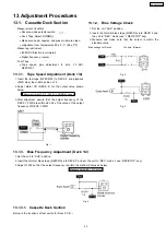
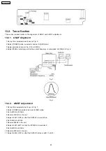
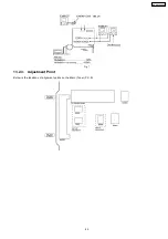


(All schematic diagrams may be modified at any time with the
development of the new technology)
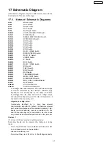
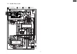
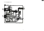
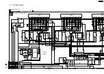
17.1. Notes of Schematic Diagrams
S951
: MODE Switch
S952
: HALF Switch
S971
: MODE Switch
S972
: HALF Switch
S975
: RECINH_F Switch
S5950
: VOLTAGE SELECTOR Switch
S6101
: POWER Switch
S6102
: SINGLE DISC CHANGE Switch
S6103
: OPEN/CLOSE Switch
S6104
: CD 1 Switch
S6105
: CD 2 Switch
S6106
: CD 3 Switch
S6107
: CD 4 Switch
S6108
: CD 5 Switch
S6201
: DECK 2 OPEN Switch
S6202
: DISPLAY/DEMO Switch
S6203
: DECK 1/2 Switch
S6204
: H.BASS Switch
S6205
: FF Switch
S6206
: REW Switch
S6207
: DECK 1 OPEN Switch
S6301
: CD Switch
S6302
: TAPE Switch
S6303
: STOP Switch
S6304
: REC Switch
S6305
: TUNER/BAND Switch
S6306
: MUSIC PORT Switch
S6307
: SUBWOOFER Switch
S6308
: MULTI DISC CHANGE Switch
S7201
: REST Switch
VR6491
: VR VOLUME JOG
VR6511
: VR MIC vOLUME JOG
·
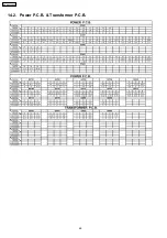
The voltage value and waveforms are the reference voltage
of this unit measured by DC electronic voltmeter (high
impedance) and oscilloscope on the basis of chassis.
Accordingly, there may arise some error in voltage values
and waveforms depending upon the internal impedance of
the tester or the measuring unit.
·
Importance safety notice :
Components
identified
by
mark
have
special
characteristics important for safety. Furthermore, special
parts which have purposes of fire-retardant (resistors), high-
quality sound (capacitors), low-noise (resistors), etc. are
used. When replacing any of components, be sure to use
only manufacturer´s specified parts shown in the parts list.
Caution !
IC, LSI and VLSI are sensitive to static electricity.
Secondary trouble can be prevented by taking care during
repair.
·
Cover the parts boxes made of plastics with aluminium foil.
·
Put a conductive mat on the work table.
·
Ground the soldering iron.
·
Do not touch the pins of IC, LSI or VLSI with fingers directly.
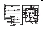
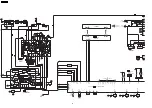
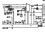
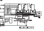
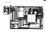
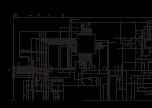
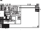
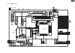
17 Schematic Diagram
57
SA-AK640GCP
Содержание SA-AK640 GBP
Страница 12: ...7 Accessories Remote Control FM Antenna Wire AC Cord AM Loop Antenna AC Plug Adaptor 12 SA AK640GCP ...
Страница 13: ...8 Operating Instructions Procedures 13 SA AK640GCP ...
Страница 14: ...14 SA AK640GCP ...
Страница 23: ...10 3 Main Parts Location 23 SA AK640GCP ...
Страница 40: ...12 2 Checking and Repairing of Transformer P C B 40 SA AK640GCP ...
Страница 41: ...12 3 Checking and Repairing of Panel Deck Deck Mechanism P C B 41 SA AK640GCP ...
Страница 42: ...12 4 Checking and Repairing of Power P C B 42 SA AK640GCP ...
Страница 47: ...47 SA AK640GCP ...
Страница 48: ...14 2 Power P C B Transformer P C B 48 SA AK640GCP ...
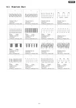
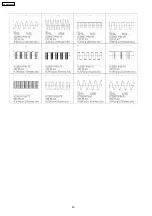
Страница 49: ...14 3 Waveform Chart 49 SA AK640GCP ...
Страница 50: ...50 SA AK640GCP ...
Страница 52: ...52 SA AK640GCP ...
Страница 58: ...58 SA AK640GCP ...
Страница 60: ...SA AK640GCP 60 ...
Страница 62: ...SA AK640GCP 62 ...
Страница 68: ...SA AK640GCP 68 ...
Страница 70: ...SA AK640GCP 70 ...
Страница 76: ...SA AK640GCP 76 ...
Страница 84: ...SA AK640GCP 84 ...
Страница 89: ...21 Exploded Views 21 1 Cabinet Parts Location SA AK640GCP 89 ...
Страница 90: ...SA AK640GCP 90 ...
Страница 91: ...21 2 Deck Mechanism Parts Location RAA4502 S SA AK640GCP 91 ...
Страница 92: ...21 3 Packaging SA AK640GCP 92 ...


