3-4
5)
Inspection on the battery voltage detector circuit
(1) Connect the keyboard to the FCR and turn on the power supply. Then finish the diagnostic program. (DOS prompt
display)
C : >
(2) Execute the inspection program for the battery voltage detector circuit.
(3) Apply DC 7.0V from the connected jigs and press an arbitrary key when the following display is presented at the LCD:
C : >input voltage = 7.0V
Press any key to continue
(4) Confirm that Battery Check = 0 is displayed at the LCD.
Input voltage = 7.0V
Press any key to continue
Battery Check = 0
(5) In the same manner, apply 7.6V, 8.2V, and 8.5V and examine the battery check value.
Input Voltage
Battery check value
7.0V
0
7.6V
2
8.2V
6
8.5V
7
3.5
Current consumption check
1) Apply the rated voltage that is specified on the main rating plate. The measured current value shall be not greater than the
rated current specified on the main rating plate.
3.6 BIOS
setup
1)
Connect the keyboard to the keyboard connector of the JS-170FR, and turn on the POWER switch.
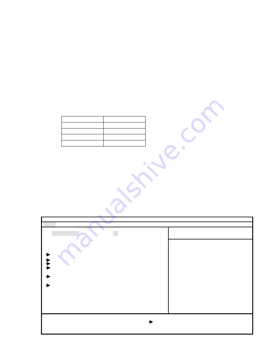
2) When the [DEL] key is pressed in the middle of POST (Power on self test) message display, a screen as shown below is
displayed.
Note)
If the BIOS setup is started for the first time, an error message may be presented in the middle of POST message
display, according to the initial condition of COMS. However, such a message shall be disregarded.
PhoenixBIOS Setup Utility
Main Advanced Power Boot Exit
Item Specific Help
System Time:
[xx:xx:xx]
System Date:
[xx/xx/xxxx]
Legacy Diskette A:
[1.44/1.25 MB 3 1/2”]
Primary Master
[****MB]
Primary Slave [None]
Secondary Master
[None]
Secondary Slave
[None]
Boot Options
Memory Cache
System Memory:
640 KB
Extended Memroy:
***** KB
<Tab>, <Shift-Tab>, or
<Enter> selects field.
F1 Help
↑↓
Select
Item -/+ Change
Values
F9 Setup
Defaults
Esc Exit
←→
Select
Menu Enter Select
Sub-Menu F10 Save
and
Exit
Содержание JS-170FR Series
Страница 2: ......
Страница 10: ......
Страница 30: ...1 20 ...
Страница 80: ...2 50 ...
Страница 101: ...3 17 LCD DISPLAY TEST 6 Video Test ENTER 1 OK or 2 NG ...
Страница 134: ...4 JS 170FR PCB s 4 1 Main PCB 4 1 1 Main PCB Schematic Diagram 1 10 4 1 ...
Страница 135: ...4 1 1 Main PCB Schematic Diagram 2 10 4 2 ...
Страница 136: ...4 1 1 Main PCB Schematic Diagram 3 10 4 3 ...
Страница 137: ...4 1 1 Main PCB Schematic Diagram 4 10 4 4 ...
Страница 138: ...4 1 1 Main PCB Schematic Diagram 5 10 4 5 ...
Страница 139: ...4 1 1 Main PCB Schematic Diagram 6 10 4 6 ...
Страница 140: ...4 1 1 Main PCB Schematic Diagram 7 10 4 7 ...
Страница 141: ...4 1 1 Main PCB Schematic Diagram 8 10 4 8 ...
Страница 142: ...4 1 1 Main PCB Schematic Diagram 9 10 4 9 ...
Страница 143: ...4 1 1 Main PCB Schematic Diagram 10 10 4 10 ...
Страница 144: ...4 1 2 Main PCB Parts Location 4 11 ...
Страница 145: ...4 2 MB PCB 4 2 1 MB PCB Schematic Diagram 4 17 ...
Страница 146: ...4 18 4 2 2 MB PCB Parts Location ...
Страница 148: ...4 3 Peripheral PCB 4 3 1 Peripheral PCB Schematic Diagram 4 20 ...
Страница 149: ...4 21 4 3 2 Peripheral PCB Parts Location ...
Страница 152: ...5 2 Main PCB 75 Peripherals ...
Страница 153: ...5 3 Power Supply Peripherals ...
Страница 154: ...5 4 Customer Display Peripherals ...
Страница 155: ...5 5 LCD Peripherals ...
Страница 156: ...5 6 Inverter PCB Peripherals ...
Страница 161: ...Printed in Japan ...


