http://cxema.ru
Order Number: MCUK980101G8
Technical Guide
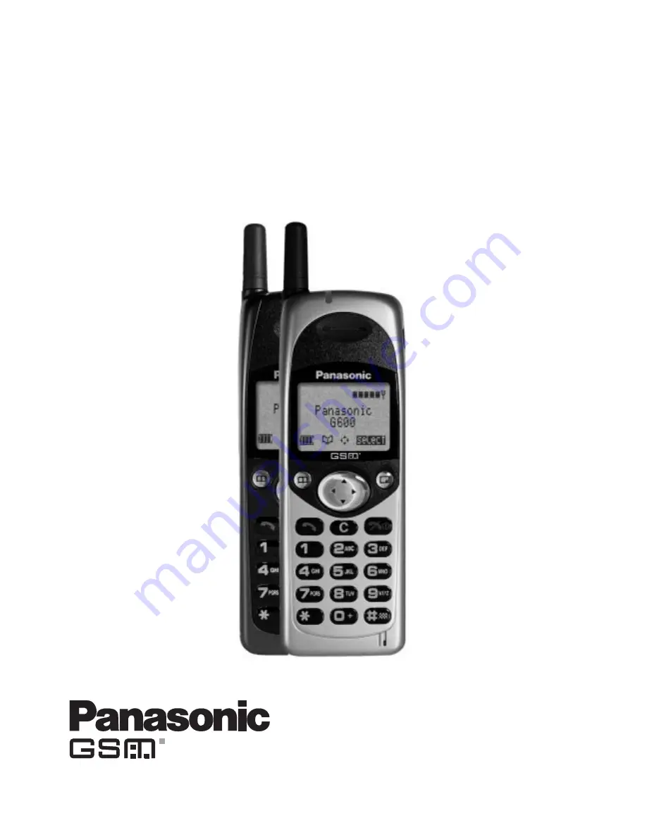
G600 Personal Cellular Telephone
Handheld portable
EB-G600
Car mount kit
EB-HF600Z
Easy fit car mount kit
Dual charger
EB-CR600
Issue 1Revision 0
Страница 1: ...xema ru Order Number MCUK980101G8 Technical Guide G600 Personal Cellular Telephone Handheld portable EB G600 Car mount kit EB HF600Z Easy fit car mount kit EB HF600Z Dual charger EB CR600 Issue 1 Revi...
Страница 2: ...or inaccuracies that may occur and reserves the right to make changes to specification or design without prior notice The information contained in this manual and all rights in any designs disclosed t...
Страница 3: ...TRANSMITTER 4 1 Introduction 4 1 4 2 Functional Description 4 2 5 RECEIVER 5 1 Introduction 5 1 5 2 Functional Description 5 2 6 BASEBAND OVERVIEW 6 1 Introduction 6 1 6 2 Functional Description 6 1 7...
Страница 4: ...ions A working area where ESDs may be safely handled without undue risk of damage from electrostatic discharge must be available The area must be equipped as follows Working Surfaces All working surfa...
Страница 5: ...ephone system are provided in the associated Service Manual 1 2 Structure of the Guide The guide is structured to provide service engineering personnel with the following technical information on the...
Страница 6: ...d Local Frequency control signal TSPACT 4 of GEMINI L RX 8 MON slot H TX slot 10 BUZZ Buzzer control signal BUZZIN of Charge IC 11 BUZZ Buzzer control signal REGFB of Charge IC 6V MAX 12 SIM RST SIM I...
Страница 7: ...O 4 of GEMINI H Ignition On L Hi Z Ignition Off 33 SERIAL_DOWN Serial Interface Downlink GEMINI USART 8251 8 bit Even 1 stop 34 nLOGIC_PWR H H power sense signal for Optional equipment LOGIC_PWR lO 1...
Страница 8: ...6 of GEMINI H TX PL5 1 L TX PL12 19 54 VBAT Battery Power Supply BAT VOLT ADIN1 10bitAD Li ION 7 2V Ni MH 4 8V 55 DCOUT 3 5V DC DC output power supply 3 44V 5 56 D5V 5 0V DC DC output power supply fo...
Страница 9: ...ut UART up 9600 33 8kbps 7 SERIAL_DOWN Output UART down 9600 33 8kbps 8 EXT_PWR Input Power for charging 9 GND Digital signal power supply ground 10 RX_AUDIO Output RX audio signal analogue 11 nRADIO_...
Страница 10: ...e BATT Battery positive BATT Battery negative S SENSE Battery Type Sensor SIM Interface PIN SIGNAL 1 GND 2 5V 3 Not connected 4 Reset 5 Serial input output 6 Clock 7 Not connected 8 Not connected MCUK...
Страница 11: ...pin 62 414 TRST U402 pin 24 415 TCK U402 pin 64 416 TMS U402 pin 61 420 VIB_ON 421 TEST 1 U402 pin 69 422 TEST 2 U402 pin 68 423 TEST 3 U402 pin 67 424 BL_VB_ON 425 CHARGE_LED 426 POLEOUT U503 pin 18...
Страница 12: ...MP 447 nADP_SENSE 448 nHF_SENSE 449 nON_HOOK 450 nLOGIC_POWER 451 IGNITION 452 SERIAL_UP 453 BATID 454 nHF_ON 455 SERIAL_DOWN 456 CHARGE_ON 457 KBC 0 458 KBC 1 459 KBC 2 460 KBC 3 461 KBC 4 462 KBR 4...
Страница 13: ...70 PARAMP 501 BUZON U501 pin 19 502 REGF8 U501 pin 15 503 nLV3 504 nRESET 505 BUZZER 506 PAGING_LED 507 EXT_PWR 508 VDD 510 VBAT 512 D5V 513 DC_OUT 514 D3V 516 A3V Issue 1 Section 2 MCUK980101G8 Revis...
Страница 14: ...11 BUZZ 13 PARAMP 15 TX_ON 16 PA_ON 17 LO_EN 18 RX_ON1 19 RX_ON2 20 nRADIO_MUTE 21 VIB_ON 22 nON_HOOK 24 BATTERY 25 DC_OUT 27 EXT_PWR 28 V_VIB 30 CKL3MI 31 SERIAL_UP 32 IGNITION 33 SERIAL_DOWN 34 nLOG...
Страница 15: ...9 DLQP 40 DLIN 41 DLIP 43 BCAL 44 IFAGCEN 45 PLL_STR 46 PLL_SD 47 PLL_CLK 49 ULQN 50 ULQP 51 ULIN 52 ULIP 53 PLL_CONT 60 AFC E901 E908 GND Issue 1 Section 2 MCUK980101G8 Revision 0 2 10 Technical Guid...
Страница 16: ...ransmit Tx and receive Rx IC s RF IF dual PLL and the antenna subsystem Figure 1 RF Block Diagram 600 0301 3 2 1 Functional Description of the PLL s The G600 design employs two fixed IF LO s 201MHz fo...
Страница 17: ...899 600 895 800 896 800 897 800 898 800 899 800 896 000 897 000 898 000 899 000 900 000 51 55 56 60 61 65 66 70 71 75 900 200 901 200 902 200 903 200 904 200 900 400 901 400 902 400 903 400 904 400 90...
Страница 18: ...e PA amplifies the output from the PA driver to any required level up to PL5 33dBm at the antenna The power level can be controlled as required in Phase II GSM in 2dB steps from 33dBm to 9dBm To achie...
Страница 19: ...the transmitter IC are given below Figure 2 Typical Losses 600 0402 MCUK980101G8 Section 4 Issue 1 Technical Guide 4 3 Revision 0 TRANSMITTER FL101 U103 FL102 U104 PA Coupler LPF FL104 2 5dB 21 5dB 2...
Страница 20: ...00 943 600 944 600 940 800 941 800 942 800 943 800 944 800 941 000 942 000 943 000 944 000 945 000 51 55 56 60 61 65 66 70 71 75 945 200 946 200 947 200 948 200 949 200 945 400 946 400 947 400 948 400...
Страница 21: ...put from the LNA goes through a differential BP SAW filter and is differentially fed into the 1st down converter mixer The LO for the mixer is generated by a PLL U304 employing a modular VCO U305 The...
Страница 22: ...levels through the receiver IC are given below Figure 2 Nominal and Worst Case Signal Levels 600 0502 102 0 105 2 90 2 94 2 89 2 98 2 Worst case dBm 102 0 104 7 87 7 90 9 82 9 91 9 Normal case dBm MC...
Страница 23: ...emissions 6 2 Functional Description The G600 baseband is based around a 2 chip GSM chipset One chip carries out signal processing with DSP and CPU called GEMINI and the other chip contains the analog...
Страница 24: ...on of a 5V step up regulator to provide the Interface requirements for a 5V SIM The SIM outputs are open drain and the inputs are 5V tolerant To achieve the required rise time on the clock line a tran...
Страница 25: ...or example 12 x 12 line or 16 x 3 line both with 2 lines of icons A Sharp LH155B display driver is used 6 2 6 Microphone The microphone is the same type used on G500 6 2 7 Buzzer The volume level of t...
Страница 26: ...code size is determined by the size of the software 7 2 2 CPU The CPU is a 32 bit RISC CPU with 16bit instruction set The CPU is designed to access 32bit memory and peripherals a further module within...
Страница 27: ...s 16 bits API RAM 0050 0000 8k CPU DSP shared ram 16 bits TPU RAM 0050 0000 8k GSM timer Microcode RAM 16 bits APIC 0050 4000 1k CPU DSP interface controller 16 bits SIM 0050 4800 1k SIM interface 16...
Страница 28: ...UART Interrupt Level sensitive IRQ_ARMIO Keypad Interrupt Low for 1 clk period IRQ_FRAME Frame Interrupt Edge sensitive IRQ_PAGE Page Interrupt Edge sensitive IRQ_TIM_GSM Edge sensitive IRQ_TSP Timed...
Страница 29: ...cted I O 12 TSPACT 0 65 TSPACT 0 I O 13 nPWRCS 56 nPWRCS I O 14 nCS1 50 PAGING_LED L Paging LED off H Paging LED On I O 15 nCS0 49 CHARGE_ON H Charger On L Charger Off 2 outputs have 6 bit PWM capabil...
Страница 30: ...t 270Kbits per second Figure 2 Functional structure of the baseband uplink path 600 0802 MCUK980101G8 Section 8 Issue 1 Technical Guide 8 1 Revision 0 VEGA TIMING JTAG 10 bit DAC SP INTERFACE Timing i...
Страница 31: ...each step being 1 16 of a bit and each step being 1 8 of a bit giving a maximum ramp time of either 14 77 S or 29 53 S An 8 bit value is used to program the ramp output level Issue 1 Section 8 MCUK98...
Страница 32: ...n GEMINI Voice Uplink path Figure 6 Voice ADC block diagram 600 0806 MCUK980101G8 Section 8 Issue 1 Technical Guide 8 3 Revision 0 VEGA 13 BIT DIGITAL MODULATOR 1 BIT DAC LOW PASS FILTER PROGRAMATION...
Страница 33: ...Type 0 136h Ni MH 137 3FFh Li ION ADC2 38 Battery Temperature 0D5h 70oC 249h 25oC 3FBh 20oC ADC3 39 nADP _SENSE 0 168h Data Adaptor 17C 1EDh RS232 Direct Cable 230 2C0h SMS Cable 2L8 365h Headset Ada...
Страница 34: ...suddenly removed primarily to protect the SIM The SIM power supply should be enabled and disabled as part of the SIM interface procedures and therefore falls outside the scope of this document Figure...
Страница 35: ...f four modes Sleep In this mode the CPU has been prevented from deactivating the linear regulators by EXT_PWR There is no CPU activity Charge The CPU is alive but may only perform battery charging fun...
Страница 36: ...is on Any other state than those in the table will cause the phone to deactivate the PSU by setting STAY_ALIVE LOW While the CPU is active it must monitor the battery condition and accessory connectiv...
Страница 37: ...600 must achieve 2 types of battery operation 4 cell Ni MH and 2 cell Li ION The power supply section consists of four parts 1 Power on circuitry 2 Voltage regulators 3 Battery charging circuitry 4 Po...
Страница 38: ...so shows a Power On Reset POR to hold the CPU in a reset state while the supply voltage and system clock stabilize Figure 2 Power supply block diagram 600 1002 MCUK980101G8 Section 9 Issue 1 Technical...
Страница 39: ...e current consumption efficiency the G600 uses 3 4V step down DC DC voltage regulators The DC DC step down circuitry uses two regulators on the LOGIC side and three regulators on the RF side to reduce...
Страница 40: ...e safeguards Deeply Discharged batteries When a battery is deeply discharged there may not be enough power to power on the phone for charging In this case the charging circuit must automatically detec...
Страница 41: ...dsfree unit via pin 4 U301 provides initial amplification of the received audio R324 is a variable resistor controlled by the thumbwheel on the side of the handsfree case providing volume level contro...
Страница 42: ...ut pin 1 Output pin 4 U305 CODEC Input pin 24 Output pin 13 U306 DSP Input pin 9 Output pin 13 U304 CODEC Input pin 12 Output pin 5 U301 Amplifier Input pin 5 Output pin 7 U312 Analogue Switch Input p...
Страница 43: ...ut E U303 and U302 5V Reg Input pin 3 Output pin 1 External Power Supply Path from P203 pin 1 Battery from car or TP203 P203 6 PIN Connector Pin 1 or TP203 D201 Diode Input pin 1 Output pin 2 Q204 PNP...
Страница 44: ...o GND J300 Pin 1 TP313 U306 pin 3 HCL U306 Pin 3 10 1 5 Adjustment and Calibration The adjustments that can be made on the handsfree unit are to the external power supply These are made by adjusting t...
Страница 45: ...istor R33 Through the potential divider R39 and R38 this turns Q5 ON turning Q16 ON Should the output CN2 become accidentally short circuited the base of Q5 becomes low turning Q5 OFF This pulls the b...