background image

7 Service Mode

7.1. Self-Diagnosis and Special Mode Setting

7.1.1. Self-Diagnosis Functions

Self-Diagnosis Function provides information for errors to service personnel by “Self-Diagnosis Display” when any error has
occurred.

U**, H** and F** are stored in memory and held.

You can check latest error code by transmitting [0] [1] of Remote Controller in Service Mode.
Automatic Display on FL will be cancelled when the power is turned off or AC input is turned off during self-diagnosis display is ON.

Error Code

Diagnosis contents

Description

Monitor Display

Automatic FL display

U30

Remote control code error

Display appears when main unit and remote
controller codes are not matched.

No display

“*” is remote controller code of the
main unit.
Display for 5 seconds.

U59

Abnormal inner temperature
detected

Display appears when the internal of drive
has abnormal temperature.
The power is turned off forcibly.
For 30 minutes after this, all key entries are
disabled. (Fan motor operates at the highest
speed for the first 5 minutes. For the
remaining 25 minutes, fan motor is also
stopped.) The event is saved in memory as
well.

No display

“U59 is displayed for 30 minutes.

U61

The unit is carrying out its
recovery process.

No display

U72

HDMI connection error
(communication error)

This error is displayed when there are any
communication problems with the unit and the
equipments (TV, amplifier etc.) connected to
the unit by HDMI. (or when there is a problem
with the HDMI cable)

U72 display disappears when
error has been solved by Power
OFF/ON of connecting equipment
or by inserting/removing of HDMI
cable.

U73

HDMI connection error
(authentication error)

When authentication error occurs while the
equipments (TV, amplifier etc.) are connected
by HDMI. (or when there is a problem with the
HDMI cable)

No display

U73 display disappears when
error has been solved by Power
OFF/ON of connecting equipment
or by inserting/removing of HDMI
cable.

U76

Injustice disc error

HDMI cannot output because you are
connected to a model that does not support
copyright protection.

No display

U88

The unit is carrying out its
recovery process.

No display

U99

Hang-up

Displayed when communication error has
occurred between Main microprocessor and
Timer microprocessor.

No display

Displayed

is

left

until

the

[POWER] key is pressed.

F00

No error information

Initial setting for error code in memory
(Error code Initialization is possible with error
code initialization and main unit initialization.)

No display

No display

F58

Drive hardware error

When drive unit error is detected, the event is
saved in memory.

No display

No display

14

DMR-EZ27P / DMR-EZ27PC

Содержание DMR-EZ27P

Страница 1: ...tsushita Electric Industrial Co Ltd All rights reserved Unauthorized copying and distribution is a violation of law Model No DMR EZ27P DMR EZ27PC Vol 1 Colour K Black Type DVD Recorder ORDER NO CHM0704014CE B24 ...

Страница 2: ...ng Parts 32 10 4 Standard Inspection Specifications after Making Repairs 33 11 Block Diagram 35 11 1 Power Supply Block Diagram 35 11 2 Analog Video Block Diagram 37 11 3 Analog Audio Block Diagram 38 11 4 Analog Timer Block Diagram 39 12 Schematic Diagram 41 12 1 Interconnection Schematic Diagram 41 12 2 Power Supply Section Main P C B 1 4 Schematic Diagram A 42 12 3 AV IO 1 4 Section Main P C B ...

Страница 3: ... potential across the resistor 4 Check each exposed metallic part and measure the voltage at each point 5 Reverse the AC plug in the AC outlet and repeat each of the above measurements 6 The potential at any point should not exceed 0 75 volts RMS A leakage current tester Simpson Model 229 or equivalent may be used to make the hot checks leakage current must not exceed 1 2 milliampere In case a mea...

Страница 4: ...ly 3 Use only a grounded tip soldering iron to solder or unsolder ES devices 4 Use only an anti static solder removal device Some solder removal devices not classified as anti static ESD protected can generate electrical charge sufficient to damage ES devices 5 Do not use freon propelled chemicals These can generate electrical charges sufficient to damage ES devices 6 Do not remove a replacement E...

Страница 5: ...2 2 Precaution of Laser Diode 5 DMR EZ27P DMR EZ27PC ...

Страница 6: ... Solder PbF The lead free solder has to be used when repairing the equipment for which the lead free solder is used Definition The letter of PbF is printed on the PCB using the lead free solder To put lead free solder it should be well molten and mixed with the original lead free solder Remove the remaining lead free solder on the PCB cleanly for soldering of the new IC Since the melting point of ...

Страница 7: ...3 Service Navigation 3 1 Service Information 3 2 Caution for DivX 7 DMR EZ27P DMR EZ27PC ...

Страница 8: ...4 Specifications 8 DMR EZ27P DMR EZ27PC ...

Страница 9: ...9 DMR EZ27P DMR EZ27PC ...

Страница 10: ...5 Location of Controls and Components 10 DMR EZ27P DMR EZ27PC ...

Страница 11: ...11 DMR EZ27P DMR EZ27PC ...

Страница 12: ...ed off 1 Turn off the power and press STOP CH UP keys on the front panel simultaneously for 5 seconds 6 1 1 2 When the power can not be turned off 1 Press POWER key on the front panel for over 10 seconds to turn off the power forcibly and press STOP CH UP keys on the front panel simultaneously for 5 seconds 6 1 2 When the Forcible Disc Eject can not be done 12 DMR EZ27P DMR EZ27PC ...

Страница 13: ...e 3 Put deck so that bottom can be seen 4 Slide SLIDE CAM by Eject Pin JZJ0484 or minus screw driver small in the direction of arrow to eject tray slightly 5 Put deck upward and push out Tray by Eject Pin JZS0484 or minus screw driver small 13 DMR EZ27P DMR EZ27PC ...

Страница 14: ... display U72 HDMI connection error communication error This error is displayed when there are any communication problems with the unit and the equipments TV amplifier etc connected to the unit by HDMI or when there is a problem with the HDMI cable U72 display disappears when error has been solved by Power OFF ON of connecting equipment or by inserting removing of HDMI cable U73 HDMI connection err...

Страница 15: ...supported format disc was played although the drive starts normally The data format is not supported although the media type is supported Exceptionally in case of the disc is dirty This disc is incompatible Display for 5 seconds NO READ Disc read error A disc is flawed or dirty A poor quality failed to start The track information could not be read Cannot read Please check the disc HARD ERR Drive e...

Страница 16: ...Lock is being set this Forced disc eject function is not accepted The display before execution leaves When the power is off press STOP and CH UP keys simultaneously for 5 seconds Forced power off When the power button is not effective while power is ON turn off the power forcibly When Schedule Recording is ON execute Forced Power off after releasing Schedule Recording Display in P off mode Press P...

Страница 17: ...keys simultaneously for 5 seconds When unlock the tray UNLOCK is displayed for 3 seconds When the power is on press STOP and POWER keys simultaneously for 5 seconds When press OPEN CLOSE key while the tray being locked Display LOCK for 3 seconds Press OPEN CLOSE key while the tray being locked ATP Initialization ATP setting and all parameters including clock are initialized and the unit turns off ...

Страница 18: ... Description Front Key Progressive initialization The progressive setting is initialized to Interlace The display before execution leaves When the power is on E E mode press STOP and PLAY simultaneously for 5 seconds 18 DMR EZ27P DMR EZ27PC ...

Страница 19: ...ut from AV Decoder Magenta picture Saturation rate 100 It is enable to switch Interlace Progressive by I P switch 1 4 Initial mode is Interlace Press 1 2 in service mode Switch Interlace Progressive Press 1 4 in Magenta Picture Output mode I P are switched alternately I P Switch Switch Interlace and Progressive in EE mode Initial setting is Interlace This command is effective during executing Whit...

Страница 20: ... Check laser used time hours of drive l is the used time display in hour lLaser used time of DVD CD in Playback Recording mode is counted Press 4 1 in service mode Delete the Laser Used Time Laser used time stored in the memory of the unit is deleted Press 9 5 in service mode 20 DMR EZ27P DMR EZ27PC ...

Страница 21: ...econds 5 Last Drive Error code No 2 1 2 is displayed for 5 seconds This Error Code is unnecessary for service 6 Last Drive Error code No 2 2 2 is displayed for 5 seconds This Error Code is unnecessary for service 7 Error occurring Disc type is displayed for 5 seconds DISC 1 DVD DISC 2 CD DISC 3 DVD RAM 2 6GB DISC 4 DVD RAM 4 7GB DISC 5 DVD R DISC Unknown Disc 8 Unused No display 9 Factor of Drive ...

Страница 22: ...ma signal and check the output on the S terminal Press 5 2 in service mode S2 signal output Forcibly superimpose the S2 signal approx 2V DC on the EE chroma signal and check the output on the S terminal Press 5 3 in service mode Front connection inspection Press all front keys and check the connection between Main P C B and Front key Switches 1 Each time a key is pressed segment turned on increase...

Страница 23: ...ating unit Second Press 6 5 in service mode Then press 0 1 1 9 the past 19 error histories are displayed Delete the Error History Delete Error History information stored on the unit Press 9 7 in service mode Tray OPEN CLOSE Test The RAM drive tray is opened and closed repeatedly Press 9 1 in service mode When releasing this mode press the POWER button of Remote Controller more than 10 seconds Erro...

Страница 24: ... C B 3 Pin Same as ES15 EH55 Series JZS0484 Eject Pin Same as EH55 EH75V ES35V Series RFKZ03D01K Lead Free Solder 0 3mm 100g Reel Same as EH55 EH75V ES35V Series RFKZ06D01K Lead Free Solder 0 6mm 100g Reel Same as EH55 EH75V ES35V Series RFKZ10D01K Lead Free Solder 1 0mm 100g Reel Same as EH55 EH75V ES35V Series RFKZ0316 Solder Remover Lead free low temperature Solder 50g Same as EH55 EH75V ES35V ...

Страница 25: ... Chart The following chart is the procedure for disassembling the casing and inside parts for internal inspection when carrying out the servicing To assemble the unit reverse the steps shown in the chart below 9 2 P C B Positions 25 DMR EZ27P DMR EZ27PC ...

Страница 26: ...9 4 Front Panel 1 Unlock 6 tabs in A F turn Pull with the front panel in the direction of your side 9 4 1 How to assemble Tray door ass y 1 Attach Blinder spring to Tray door ass y 2 Attach Tray door ass y in order from to Put the Brinder spring on the groove Insert the shaft in the hole Insert the shaft in the hole 3 Confirm the Brinder spring is attached as following 26 DMR EZ27P DMR EZ27PC ...

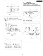
Страница 27: ...k SD Card P C B CAUTION When replacing Digital P C B pay attention as below 9 6 Rear Panel 1 Remove 6 Screws A and 2 Screws B 2 Unlock 2 Locking Tabs A to remove Rear Panel 9 6 1 Only Fan Motor 1 Remove the 2 Screws C and connector remove the Fan motor 27 DMR EZ27P DMR EZ27PC ...

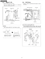
Страница 28: ...move Digital P C B CAUTION When replacing Digital P C B pay attention as below 9 8 DVD Drive 1 Remove 3 Screws A and wire with connector to remove DVD Drive Caution when assembling DVD drive When assembling DVD drive draw around wire with connector between capacitors on Main P C B as following 28 DMR EZ27P DMR EZ27PC ...

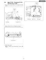
Страница 29: ...B and Front L P C B 1 Remove 4 Screws A to remove Front angle and Front jack P C B 2 Remove Front L P C B in the direction of arrows 3 Remove Drive angle Remove 4 Screws A and Rear angle to remove Main P C B 29 DMR EZ27P DMR EZ27PC ...

Страница 30: ...10 Measurements and Adjustments 10 1 Service Positions Note For description of the disassembling procedure see the section 9 10 1 1 Checking and Repairing Digital P C B 30 DMR EZ27P DMR EZ27PC ...

Страница 31: ...10 1 2 Checking and Repairing of Main P C B 31 DMR EZ27P DMR EZ27PC ...

Страница 32: ... replacing Digital P C B TM L1 is displayed after replacing Digital P C B Once power off and start up again 10 3 Caution for Replacing Parts 10 3 1 Items that should be done after replacing parts 32 DMR EZ27P DMR EZ27PC ...

Страница 33: ...t to establish the judgement criteria for the picture and sound Item Contents Check Item Contents Check Picture Block noise Sound Distorted sound Crosscut noise Noise static background noise etc Dot noise The sound level is too low Picture disruption The sound level is too high Not bright enough The sound level changes Too bright Flickering color Color fading 33 DMR EZ27P DMR EZ27PC ...

Страница 34: ...34 DMR EZ27P DMR EZ27PC ...

Страница 35: ... VA1101 L1101 ABSORBER SURGE AND SUPPRESSOR SURGE F1101 P1101 AC SOCKET DMR EZ27P PC Power Supply Block Diagram H H H H H Audio Main Section Audio Main Section ON REG ANA 3 3V ANA 3 3V 8 5 1 VIN VOUT IC1500 30 IC7501 3 CONT 2 CONT ON ON IC4001 VOUT VIN 5 1 4 REG AU 9V IC4003 1 VIN IC1510 5 REG X SW 5 2V X SW 5 2V VOUT DI P ON 23 7 POWER TRANS T7501 1 2 IP7501 1 REG AU 5V IC4002 4 3 5 VIN VOUT IC49...

Страница 36: ...001 1 4 12 14 17 25 40 44 45 49 52 53 64 72 78 PFAIL IC7501 29 2 IC7514 VDD OUT PFAIL OUT 1 XRESET 4 X RESET VOUT VDD IC7512 5 IC7501 8 X SW 4V X SW 4V 37 P7401 P56001 D 3 3V 41 43 P7401 P56001 ANA 3 3V 33 P7401 P7401 P56001 47 49 51 P7401 P59001 21 P56001 D 5V D 5V 25 P7401 P56001 X SW 12V X SW 12V K UNREG38V 55 P56001 P7401 19 P56001 P7401 72 AU 5V AU 5V X SW 5 2V P56001 P7401 29 P56001 P7401 E ...

Страница 37: ...ION TO DIGITAL Y V OUT A COUT A 65 69 42 P56001 P7401 V YIN DM 38 P56001 P7401 CPNCIN DM RPC R OUT BPC B OUT GPC Y OUT CPN Y OUT CPS V OUT CPN C OUT C S DET CPN Y IN CPN C IN LINE V IN 480P 480I VIDEO OUT COMPONENT JK3903 19 IC7501 8 DET OUT A S1 S2 OUT 31 RED PR CR BLUE PB CB Y GREEN 2 3 4 VIDEO OUT JACK A V OUT JK3901 10 9 13 OUT S VIDEO C Y C S DET1 Y1 IN C1 IN VIDEO1 IN C S DET3 Y3 IN C3 IN VI...

Страница 38: ... P56001 30 P7401 OPTICAL 1 DIGITAL AUDIO OUT IC4901 SECTION DIGITAL BLOCK FROM 22 P56001 P7401 IECOUT LOUTL LOUTR 16 19 AUDIO L R 86 P56001 P7401 MIXROUT DM 84 P56001 P7401 MIXLOUT DM 100 XTMUTE Q4003 MUTE MUTE Q4004 QR4001 4002 4003 MUTE 68 P56001 P7401 XDMUTE AUDIO PROCESSOR SDA SCL FRONT2 FRONT1 EXT22 EXT21 31 32 12 11 21 20 2 AUDIO L R FRONT R IN FRONT A V IN JACK JK3801 5 3 FRONT L IN R IN L ...

Страница 39: ...48 S18 47 44 G4 G1 CH UP S7507 S7502 PLAY IC7501 TIMER FRONT L P C B IR7501 1 3 2 L123 SWIDE XT MUTE 10MHz OUT 10MHz IN DI P ON KEY3 IR KEY2 KEY1 19 39 100 10 11 7 23 18 RST KEY 37 25 17 16 DP7501 DISPLAY TIMER MAIN CLK 10MHz X7501 X SW 12V DI P ON JC P ON H H DR P ON 71 DR P ON BLOCK SECTION FROM VIDEO XT MUTE BLOCK SECTION TO DIGITAL HDMI P ON H HDMI P ON H BLOCK SECTION POWER TO S1 S18 G1 G4 S7...

Страница 40: ...DMR EZ27P DMR EZ27PC 40 ...

Страница 41: ...D I2C5CK X SW 5 8V DGND DGND I2C5DT D5V DGND DGND IECOUT DI PON DL H DGND DI PON H XFWE HDMI P5 ON H XMPREQ DGND SBPTM DGND DGND DGND SBMTP HDMI CONT XINTM DGND SCLK HDMI MONI XINTP DGND UART2 RX UART2 TX AUGND TU SDA MIXROUT DM DGND MIXLOUT DM TU SCL AUGND DGND AADC R TU IF OUT1 AADC L DGND AUGND TU IF OUT2 AUGND DGND AU5V TU IF AGC AUGND DGND XDMUTE X SW2 3V DGND DGND 88 87 86 85 84 83 82 81 80 ...

Страница 42: ...01 C1502 C1501 6 3V1 8200 R1500 C1503 10 1800 R1501 D1502 MA2C700A0F 1 C1510 6 7 5 2 4 3 8 1 C0CBCBD00048 IC1500 C1500 10V1 3 1 2 4 5 C0CBCDC00054 IC1510 1 C1511 2 1 4 3 P1500 TO RAM DRIVE K1KA04AA0180 G0A100HA0023 L1271 K1530 VWJ0795 15 CL1504 VWJ0795 5 K1260 D1500 B0EAKL000062 C1261 10V220 VWJ0795 5 K1270 CL1501 CL1503 B0EAKL000062 D1501 L1280 G0A220GA0026 D1280 B0JAQE000004 10V680P C1280 10V100...

Страница 43: ...IN VOUT NC GND CNT 4 2 3 1 5 IC VIN SUB ON H VOUT GND NC CN SHUTDOWN THERMAL LIMITTER CURRENT DRIVER BIAS REFERENCE 7 1 3 2 4 5 6 IC1150 SWITCHING IC IC DETAIL BLOCK DIAGRAM IC1510 XSW 5 2V SWITCHING REGULATOR IC DETAIL BLOCK DIAGRAM IC1500 ANA 3 3V SWITCHING REGULATOR IC DETAIL BLOCK DIAGRAM IC1530 D 5V SWITCHING REGULATOR IC DETAIL BLOCK DIAGRAM IC1520 DC DC CONVERTER IC DETAIL BLOCK DIAGRAM IC1...

Страница 44: ...7410 CL7467 CL7459 CL7441 G0A100HA0023 L7400 CL7447 CL7485 0 LB7405 LB7412 0 CL7425 HDMI_CONT ANA3R3V D3R3V T1R5V G_TUIFOUT2_A G_TUIFOUT1_A G_TU_SDA_A G_TU_SCL_A D2R3V G_TU_IFAGC_A X_SW_3R2V X_SW_4V HDMI_P5_ON_H D5V HDMI_MONI EXT31 TU TU NC CAP1 EXT12 EXT11 TUOL TUOR EXT22 EXT21 SCL DAR LOUTR REGFIL OUTR DAL LOUTL SDA GND DGND DGND DGND DGND XFWE DGND DGND DGND DGND DGND DGND DGND D3R3V X_SW_5R8V ...

Страница 45: ...020 1K C4019 50V1 C4020 50V1 R4024 100K R4023 100K C4018 16V220P C4017 0 1 ZF R3922 75 220 R4043 680 R4037 25V47 C4026 11 7 9 8 1 3 5 13 4 12 15 20 18 19 21 16 17 14 2 6 10 JK3901 K2HE219B0004 K1U822B00003 NC C CPS L OUT C CPN L IN Y UNR5111 TX NC or LINE IN R LINE OUT L CPS L IN LINE IN L LINE OUT R T P TUIL TUIR OUTL Y P P IN GND VCC P UNR5211 TX GND NR VOUT PQ1L503M2SPQ or ON H NR GND ON H VIN ...

Страница 46: ...1 12 14 15 16 B 8 9 10 7 6 E F G D C 5 4 3 2 1 B A DMR EZ27P PC AV IO 3 4 Section Main P C B 2 4 Schematic Diagram A TO AV IO SECTION 1 4 LOCATION MAP 1 4 2 4 3 4 4 4 B NOTE DO NOT USE THE PART NUMBER SHOWN ON THIS DRAWING FOR ORDERRING THE CORRECT PART NUMBER IS SHOWN IN THE PARTS LIST AND MAY BE SLIGHTLYDIFFERNT OR AMENDED SINCE THIS DRAWING WAS PREPARED P Power Supply Section Page A A AV IO Sec...

Страница 47: ... IN PY G OUT PY G SAG DRV GND1 PB B SAG DRV VCC1 Y75 SAG Y75 OUT TEST1 CLKR SYN GND CLK MONI SLICE DC SCL SDA AV2 B IN DRV VCC3 VREG SYNC_CR VREF AV2 G IN TEST2 C OUT A LINE 3 OUT 59 SYNC DET OUT LINE 2 OUT SLICER VIDEO A SGND C OUT B SW GND1 SW VCC1 78 DVCC2 80 TEST3 79 BLSW OUT SLICER VIDEO B Y V OUT B DVD B PB IN SYN VCC Y V OUT A 60 V C SYNC OUT 42 DRV GND3 41 DVD C IN 21 Y 3 IN 22 DRV GND2 23...

Страница 48: ... IN VIDEO1 IN TUNER 6 7 10 5 20 21 24 19 3 35 43 51 33 47 36 37 39 27 26 29 28 30 41 27 24 OUTR RFOUT 26 DAL DAR 25 0 5dB 0 5dB SELECTOR INPUT 6 1dB 6 1dB 2 LOGIC BUS I C EXT12 10 EXT11 9 LS OUTL 28 29 SDA SCL FRONT2 FRONT1 EXT22 EXT21 31 32 12 11 21 20 H VIN VOUT NR GND ON 1 2 3 4 5 IC H NOISE GND ON VOUT VIN REFERENCE BANDGAP PROTECTION THERMAL 5 4 3 2 1 IC3001 VIDEO PROCESSOR IC DETAIL BLOCK DI...

Страница 49: ... 14 16 18 20 23 22 24 21 19 17 15 12 13 IC7301 C1AB00002666 RFC_SW RFC_5V AUDIO_IN BOOSTER_5V TU_MONITOR NC SIF_OUT VIF_5V VIDEO_OUT AFT 30V TUNER_5V IFD_OUT2 IFD_OUT1 IF OUT IF_AGC IIC_CLK IIC_SDA VIDEO_IN AGC RFC_ON OFF VCC LOUT PCREG PCSPE PCTIM ROUT PCKE6B SDA ADDSET SCL ST_SAP GND PCFIL POSIF SAPDET PCDET DBXIN PCTNWID PCDCIN or STPDET VO GND CONT VIN CN or PCPLC STPLL PCDCOUT P A A A T A T A...

Страница 50: ... 70 69 73 75 10 8 7 9 12 11 99 100 95 94 96 97 90 91 89 93 92 98 4 6 5 2 1 3 81 82 80 86 87 88 84 83 85 45 19 17 15 14 16 18 43 23 21 20 22 41 24 39 37 33 35 34 29 30 27 26 28 32 31 36 38 25 40 42 44 46 IC7501 MN67789CA C7508 0 01 C7507 0 01 XSW_5V_T 1 2 JW7501 TO FRONT L P C B VWJ02H5065VV UART2RX R7602 2200 S7505 EVQ11A04M EVQ11A04M S7507 EVQ11A04M S7503 R7601 1500 EVQ11A04M S7502 S7501 EVQ11A04...

Страница 51: ...T MUTE 100 71 JC P ON H 7 DIP ON H DR P ON H 23 P SAVE H P FAL L 29 IR REMOCON 25 XC OUT 14 XC IN 13 PS GND VDD VOUT 4 2 5 Vref 1 GND VDD OUT 1 3 2 Vref 8 7 6 5 1 2 3 4 B IN B IN BOUT V GND A IN A IN AOUT IC7501 TIMER IC DETAIL BLOCK DIAGRAM IC7512 X RESET IC DETAIL BLOCK DIAGRAM IC7514 RESET IC DETAIL BLOCK DIAGRAM IC7504 FAN MOTOR DRIVE IC DETAIL BLOCK DIAGRAM IC7501 Detail Block Diagram IC7504 ...

Страница 52: ... 8 1 3 4 2 20 19 P66802 TO P56501 DIGITAL P C B AVENC RTSC AVDEC MAIN CPU 2 K1MY20AA0021 2 1 4 3 P66803 DV JACK K1FY104B0006 TPB TPB CLK GND WP GND CMD COM DAT1 DAT3 FG SD CARD DAT2 3R3V DAT0 TPA CD FG TPA GND D3R3V DAT2 D3R3V TPA WP GND CMD DAT3 GND TPB TPA GND TPB GND CD DAT1 DAT0 GND CLK 8 9 10 7 6 E F G D C 5 4 3 2 1 B A DMR EZ27P PC DV Jack SD Card Schematic Diagram NOTE DO NOT USE THE PART N...

Страница 53: ...2HA307A0011 6 4 2 5 3 1 K1CB104A0017 JK3802 75 R3928 R3929 75 C3907 0 1 R3927 75 0 01 C3908 5 6 1 3 4 2 8 7 AV IO SECTION TO MAIN P C B LB3915 J0JCC0000103 LB4911 J0JCC0000103 LB4912 J0JCC0000103 1K R3926 J0JCC0000103 LB3914 LB3913 J0JCC0000103 ZJ3901 K9ZZ00001279 OR FRONT_C_IN GND AUGND FRONT_V_IN FRONT_Y_IN FRONT_S_IN_L FRONT_R_IN FRONT_L_IN 5 4 3 2 1 A B DMR EZ27P PC Front Jack Schematic Diagra...

Страница 54: ...DMR EZ27P DMR EZ27PC 54 ...

Страница 55: ... Circuit Board 13 1 Main P C B 13 1 1 Main P C B 1 4 Section 1 A B C D 2 3 4 5 1 4 2 4 3 4 4 4 DMR EZ27P PC Main P C B VEP79141A EZ27P VEP79141B EZ27PC 1 4 Section Location Map FRONT REAR DMR EZ27P DMR EZ27PC 55 ...

Страница 56: ...13 1 2 Main P C B 2 4 Section HOT COLD 5 6 7 8 9 1 4 2 4 3 4 4 4 DMR EZ27P PC Main P C B VEP79141A EZ27P VEP79141B EZ27PC 2 4 Section Location Map FRONT REAR DMR EZ27P DMR EZ27PC 56 ...

Страница 57: ...13 1 3 Main P C B 3 4 Section C D E F Main P C B 1 4 2 4 3 4 4 4 DMR EZ27P PC Main P C B VEP79141A EZ27P VEP79141B EZ27PC 3 4 Section Location Map FRONT REAR DMR EZ27P DMR EZ27PC 57 ...

Страница 58: ...13 1 4 Main P C B 4 4 Section HOT COLD 1 4 2 4 3 4 4 4 DMR EZ27P PC Main P C B VEP79141A EZ27P VEP79141B EZ27PC 4 4 Section Location Map FRONT REAR DMR EZ27P DMR EZ27PC 58 ...

Страница 59: ...L7501 F 7 C1520 C 5 C4013 B 3 C7524 E 7 R3006 D 3 R7407 D 4 R7592 C 4 Q7509 E 6 TL7507 E 4 LB1103 C 6 C1521 C 5 C4014 B 3 C7525 E 6 R3007 D 3 R7408 D 4 R7599 E 5 Q7801 B 5 LB1104 C 6 C1522 C 5 C4017 C 3 C7527 F 7 R3009 D 2 R7501 E 6 R7600 F 5 Q7802 E 6 JK3901 A 3 LB1105 D 7 C1523 C 5 C4018 C 3 C7530 F 6 R3011 E 2 R7503 F 7 R7601 F 5 JK3903 A 4 LB1150 C 7 C1524 C 5 C4019 C 2 C7531 F 7 R3901 A 3 R75...

Страница 60: ...2 Front L P C B 1 A B C D 2 3 4 5 DMR EZ27P PC Front L P C B VEP73142A Front L P C B 13 3 Front Jack P C B 1 A B C D 2 3 4 5 DMR EZ27P PC Front Jack P C B VEP73143A Front Jack P C B DMR EZ27P DMR EZ27PC 60 ...

Страница 61: ...rd P C B 1 A B C D 2 3 4 5 6 7 8 9 DV Jack SD Card P C B Foil Side DMR EZ27P PC DV Jack SD Card P C B Foil Side VEP73144A Component Side DMR EZ27P PC DV Jack SD Card P C B Component Side VEP73144A DMR EZ27P DMR EZ27PC 61 ...

Страница 62: ...DMR EZ27P DMR EZ27PC 62 ...

Страница 63: ...1 4 0 0 1 2 7 4 9 1 8 1 8 1 9 1 9 2 2 0 2 2 2 2 2 2 2 2 1 7 1 7 0 1 8 5 0 Ref No MODE 41 42 43 44 45 46 47 48 49 50 51 52 53 54 55 56 57 58 59 60 REC 2 8 0 2 8 4 9 4 9 2 8 1 8 4 9 0 2 8 4 9 4 9 2 9 1 1 0 5 1 5 1 5 1 0 1 PLAY 2 8 0 2 8 4 9 4 9 2 8 1 8 4 9 0 2 8 4 9 4 9 2 9 1 1 0 5 1 5 1 5 1 0 1 STOP 2 8 0 2 8 4 9 4 9 2 8 1 8 4 9 0 2 8 4 9 4 9 2 9 1 1 0 5 1 5 1 5 1 0 1 Ref No MODE 61 62 63 64 65 66 ...

Страница 64: ...6 12 4 2 3 2 3 0 0 0 3 0 0 0 3 Ref No MODE E C B E C B E C B E C B REC 0 4 9 0 0 9 1 0 2 0 0 2 0 4 5 1 12 4 5 5 PLAY 0 4 9 0 0 9 3 0 1 0 0 1 0 4 5 1 12 4 5 5 STOP 0 4 9 0 0 9 1 0 2 0 0 2 0 4 5 1 12 4 5 5 Ref No MODE E C B E C B REC 2 6 0 2 0 0 0 1 0 6 PLAY 2 6 0 2 0 0 0 1 0 6 STOP 2 6 0 2 0 0 0 1 0 6 Ref No MODE E C B E C B E C B E C B E C B REC 0 0 2 3 5 1 0 2 5 1 0 5 1 0 0 0 4 9 36 7 36 7 0 1 PL...

Страница 65: ...c div IC1150 2 STOP 0 5Vp p 5 sec div P7401 64 REC PLAY 1 0Vp p 20 sec div JK3903 2 REC PLAY 1 0Vp p 20 sec div JK3903 4 REC PLAY 2 0Vp p 20 sec div JK3903 3 REC PLAY 1 0Vp p 20 sec div P7401 42 REC PLAY 1 0Vp p 20 sec div P7401 48 REC PLAY 0 6Vp p 20 sec div P7401 52 REC PLAY 1 0Vp p 20 sec div P7401 56 REC PLAY 0 6Vp p 20 sec div P7401 60 REC PLAY 0 8Vp p 20 sec div P7401 78 80 REC PLAY 0 8Vp p ...

Страница 66: ...RTH H HA0 UP HD0 UP HINT HRXW HOST ADDRESS HOST DATA HOST INTERRUPT HOST READ WRITE INITIAL LOGO ABBREVIATIONS I IECOUT IPFRAG IREF ISEL IEC958 FORMAT DATA OUTPUT INTERPOLATION FLAG I CURRENT REFERENCE INTERFACE MODE SELECT L LDON LPC LRCK LASER DIODE CONTROL LASER POWER CONTROL L CH R CH DISTINCTION CLOCK M MA0 UP MCK MCKI MCLK MDATA MDQ0 UP MDQM MLD MPEG MEMORY ADDRESS MEMORY CLOCK MEMORY CLOCK ...

Страница 67: ... BACK VOLTAGE REFERENCE SOURCE POWER SUPPLY VOLTAGE W WAIT WDCK WEH WSR BUS CYCLE WAIT WORD CLOCK WRITE ENABLE HIGH WORD SELECT RECEIVER X X XALE XAREQ XCDROM XCS XCSYNC XDS XHSYNCO XHINT XI XINT XMW XO XRE XSRMCE XSRMOE XSRMWE XVCS XVDS XVSYNCO X TAL X ADDRESS LATCH ENABLE X AUDIO DATA REQUEST X CD ROM CHIP SELECT X CHIP SELECT X COMPOSITE SYNC X DATA STROBE X HORIZONTAL SYNC OUTPUT XH INTERRUPT ...

Страница 68: ...15 Parts and Exploded Views 15 1 Exploded Views 15 1 1 Casing Parts Mechanism Section 68 DMR EZ27P DMR EZ27PC ...

Страница 69: ...15 1 2 Packing Accessories Section 69 DMR EZ27P DMR EZ27PC ...

Страница 70: ...TOR 1 n n n n VEP79141A MAIN P C B 1 RTL P n n n n VEP79141B MAIN P C B 1 RTL PC C1101 ECQU2A683MLC 0 068U 1 C1102 F1B2G1020002 1000P 1 C1103 F1B2G1020002 1000P 1 C1104 ECQU2A223MLC 0 022U 1 C1107 F2B2E1010002 250V 10P 1 C1108 F1B2G1020002 1000P 1 C1150 F2A1V5600013 35V 56U 1 C1151 F1B3A182A009 250V 1800P 1 C1152 ECJ1VB1H102K 50V 1000P 1 C1153 ECJ1VC1H101J 50V 100P 1 C1154 F1H1H222A798 50V 2200P 1...

Страница 71: ...ECJ1VB1H103K 50V 0 01U 1 C7510 ECJ1VC1H180J 50V 18P 1 C7511 F1H1H150A799 50V 15P 1 C7512 ERJ3GEY0R00V 1 10W 0 1 C7514 F1H1C104A071 16V 0 1U 1 C7516 F1H1C104A071 16V 0 1U 1 C7520 F1H1C104A071 16V 0 1U 1 C7521 ECJ1VC1H101J 50V 100P 1 Ref No Part No Part Name Description Pcs Remarks C7522 F2A0J470A824 6 3V 47P 1 C7523 F1H1A105A028 10V 1U 1 C7524 F2A1H100B040 50V 10P 1 C7525 ECJ1VB1H103K 50V 0 01U 1 C...

Страница 72: ... TRANSISTOR 1 Q7503 2SD0601A0L TRANSISTOR 1 Q7509 B1ABMD000004 TRANSISTOR 1 Q7801 2SB1218A0L TRANSISTOR 1 Q7802 2SD1819A0L TRANSISTOR 1 QR4001 UNR521100L TRANSISTOR 1 QR4002 UNR511100L TRANSISTOR 1 QR4003 UNR521100L TRANSISTOR 1 QR7401 UNR521300L TRANSISTOR 1 QR7801 UNR511200L TRANSISTOR 1 R1150 ERJ6GEYJ100V 1 8W 10 1 R1151 ERJ6GEYJ100V 1 8W 10 1 R1152 ERJ3GEYJ103V 1 10W 10K 1 R1153 ERJ3GEYJ752V 1...

Страница 73: ...31T 1 4W 330 1 R7546 ERDS2TJ1R0T 1 4W 1 0 1 R7547 ERJ3GEYJ101V 1 10W 100 1 R7548 ERJ3GEYJ103V 1 10W 10K 1 R7549 ERJ3GEYJ473V 1 10W 47K 1 R7550 ERJ3GEYJ562V 1 10W 5 6K 1 R7551 ERJ3GEYJ470V 1 10W 47 1 R7552 ERJ3GEYJ473V 1 10W 47K 1 Ref No Part No Part Name Description Pcs Remarks R7553 ERJ3GEYJ473V 1 10W 47K 1 R7556 ERJ3GEYJ101V 1 10W 100 1 R7557 ERJ3GEYJ101V 1 10W 100 1 R7565 ERJ3GEYJ103V 1 10W 10K...

Страница 74: ...1 RTL 4 VEP79141A MAIN P C B 1 RTL P 4 VEP79141B MAIN P C B 1 RTL PC 5 RFKB79142B DIGITAL P C B 1 RTL 6 L6FAJCCH0007 FAN MOTOR 1 7 RGR0364D A1 REAR PANEL 1 P 7 RGR0364D B1 REAR PANEL 1 PC 8 RHD30111 3 SCREW 13 9 RHD30119 L SCREW 13 10 RHD30151 SCREW 2 11 RMA2047 FRONT ANGLE 1 12 RMA2048 DRIVE ANGLE 1 13 RMA2049 REAR ANGLE 1 14 RKA0144 K FOOT RUBBER 5 15 RMZ0825 1 SHEET 2 16 VEE1D24 WIRE WITH CONNE...

Отзывы: