background image


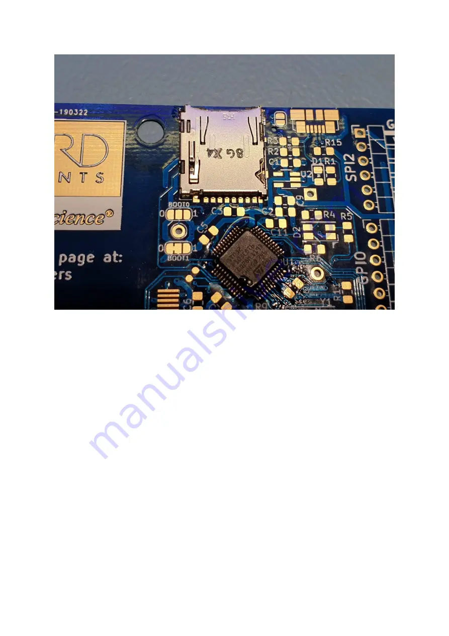
Solder down the tab on the top left of the package to ensure it is firmly held in place. Apply flux to 
the data pins at the base of the package and then apply the soldering iron and a small amount of 
solder to each pin one at a time. Ensure there are no shorts between pins, or between any of the 
pins and the metal body of the SD card socket. Use extra flux and solder wick to remove any excess 
solder from any bridged pins. 

Solder the remaining pins on the right hand side of the package and then, while wearing gloves, 
repeat the cleaning process described in step 1. 

Содержание STM32F103C8T6

Страница 1: ...dsyn soldasip Acetone or isopropyl alcohol IPA for washing Latex or nitrile gloves to be worn during wash operations Double sided tape to mount the display ChipQuik de soldering alloy optional needed...

Страница 2: ...er bridges 2 or 3 pins together as this will be corrected later Solder down a pin on the opposite side of the processor ensuring the alignment is exactly correct This will hold the processor in place...

Страница 3: ...more flux clean the iron and try running it along the pins again The solder on the tip of the iron became oxidised clean the iron re apply solder and work quickly to avoid oxidisation The soldering i...

Страница 4: ...ise when the solvent flashes off the flux will remain on the PCB Step 2 The SD card socket The SD card socket is the next hardest component to solder and so should be tackled next First tin the pad in...

Страница 5: ...a small amount of solder to each pin one at a time Ensure there are no shorts between pins or between any of the pins and the metal body of the SD card socket Use extra flux and solder wick to remove...

Страница 6: ...Step 3 The USB Socket Tin the top right pad of the USB socket PCB footprint and position the USB socket correctly over its footprint Use the soldering iron to stick the USB socket to the tinned pad...

Страница 7: ...hen apply a small amount of solder to each pin one at a time and then while wearing gloves repeat the cleaning process from steps 1 and 2 Ensure there are no shorts between pins or between any of the...

Страница 8: ...d by matching the pin 1 indicator on top of the package with the marking on the PCB Use the soldering iron to stick the part to the tinned pad Once the part is soldered in place press on the top of th...

Страница 9: ...this component is to place it onto the untinned pads as shown in the image above Apply the soldering iron to the exposed section of one of the pads and apply solder The solder will wick under the cry...

Страница 10: ...g iron and a small amount of solder to each of the remaining pins one at a time The power LED PCB footprint has an arrow showing the proper orientation of the component The LED has an arrow on the und...

Страница 11: ......

Страница 12: ...l the 0805 footprints at the same time on the PCB Refer to the bill of materials to determine which values of resistor and capacitor should be fitted where Each component is marked with a reference de...

Страница 13: ......

Страница 14: ......

Страница 15: ...fresh solvent It is important to dry the PCB with paper towel rather than just letting the solvent evaporate If the solvent is just allowed to dry any dissolved flux residue will remain on the PCB aft...

Страница 16: ...circuits between pins on the display connector after soldering This can be done with a multi meter in continuity mode Note that pins 5 and 6 are intentionally connected together near C6 Once all the p...

Страница 17: ......

Страница 18: ......

Страница 19: ...er switch is a set of pads suitable for bypassing the switch to hard wire the PCB for USB or battery operation without fitting the switch Pads are also available for this purpose on the top surface of...

Страница 20: ......

Отзывы: