


NB3N1200KMNGEVB, NB3W1200LMNGEVB
http://onsemi.com
7
Graphical User Interface (GUI)
USB & I
2
C/SMBus Interface
The NB3N1200K EVB has an on-board I
2
C/SMBus
interface circuitry located in the upper left section of the
board.
This circuitry will interface with the software program
and the device via the SDA and SCL input pins, and can
control all twelve of the OE_n# pins, PLL Mode and
Frequency Select directly from the GUI.
SCL & SDA
The SMBus Clock (SCL) and Data (SDA) pins are
exercised through the on-board I
2
C interface.
In order to enable the I
2
C control of the DUT, header
jumpers J63 & J64 must be shorted.
The I
2
C/SMBus interface circuitry is powered separately
from the USB type-B connection and is isolated from device
VDD and VDDIO.
The SDA and SCL pins can also be externally accessed by
an off-board programmer, allowing other SMBus emulators
to be used to program the DUT. If used, remove both jumpers
J63 & J64. “Test-point anvils” TP5 & TP6 are available for
external control of the device with the use with mini-grabber
cables.
BOARD FEATURES
Single Board Design/Layout for NB3N1200K or
NB3W1200L:
•
The single board design and layout accommodates the
electrical characterization of either the NB3N1200K
(standard HCSL outputs) or the NB3W1200L (HCSL
Push-Pull outputs).
•
Incorporates on-board I
2
C/SMBus interface circuitry
powered from a USB connection, minimizing cabling.
•
Convenient and compact board layout.
•
3.3 V power supply device operation.
•
Differential inputs/outputs signals are accessed via
SMA connectors or high impedance probes.
Other Board Features
There are no vias on the high-speed differential I/O metal
traces so as to eliminate via impedance and stub affects.
Board stand-offs are installed.
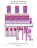
Board Layout
The NB3N1200K QFN-64 Evaluation Board provides
a high bandwidth, 50-
W
controlled trace impedance
environment (100-
W
line-to-line differential) and is
implemented in four layers.
•
All layers are constructed with FR4 dielectric material.
•
The first layer is the primary signal layer, including all
of the differential inputs and outputs.
•
The second layer is the ground plane. It is dedicated for
the DUT ground/SMA ground plane.
•
The third layer is dedicated as the power plane.
A portion of this 3
rd
layer is designated for the device
VDD and VDDIO power planes.
•
The fourth layer contains control lines, power supply
banana jacks and device power pin bypass capacitors.
Layer Stack
•
L1 (Top) Signal
•
L2 Device Ground and SMA Ground
•
L3 VDD, VDDIO (Separate Device Power Supplies)
•
L4 (Bottom), Power Supply By-pass Capacitors,
Control Pin Traces and Banana Jacks
Figure 11. NB3N1200KMNGEVB and NB3W1200LMNGEVB Evaluation Board Layer Stack-Up