


TWR-KL28Z Hardware Description
TWR-
KL28Z User’s Guide, Rev. 0, 06/2016
8
NXP Semiconductors
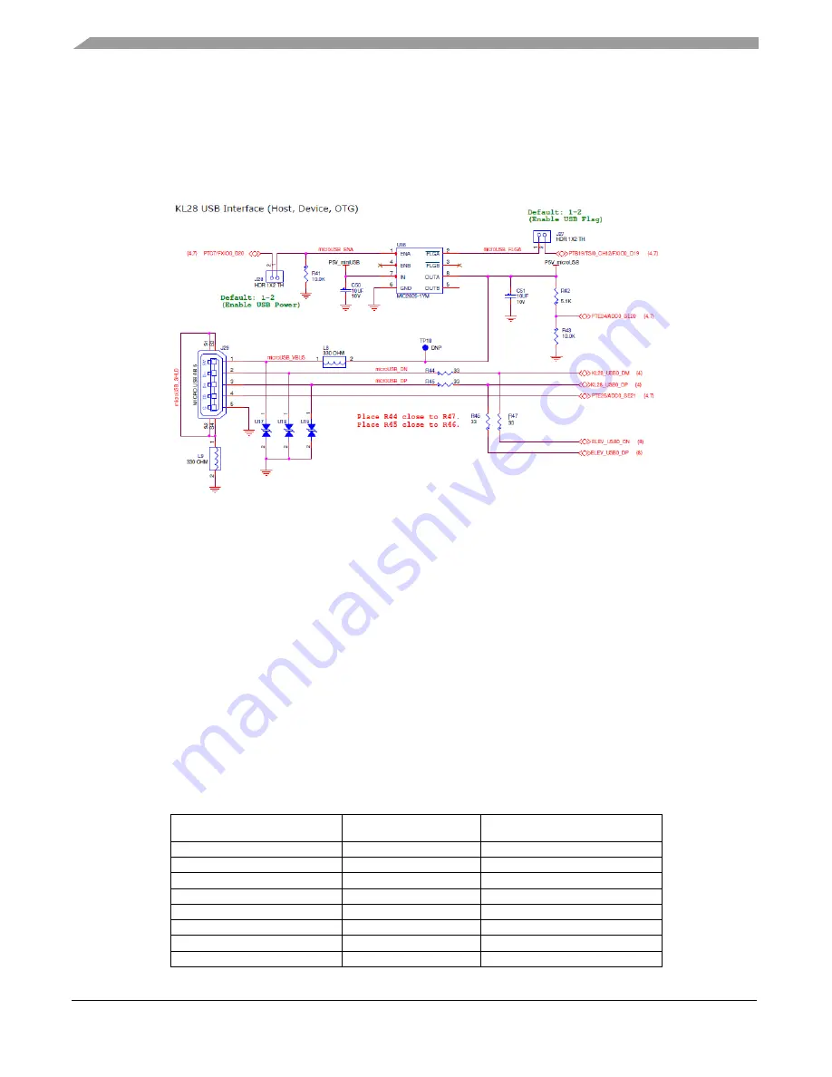
4.3.3. USB port
The Kinetis KL28 microcontrollers feature a dual-role USB controller with on-chip full-speed and low-
speed transceivers. The USB interface on the TWR-KL28Z is configured as a full-speed USB device.
J29 is the USB connector for this interface
.
As shown in
Figure 6
.
Figure 6. USB connector schematic
4.3.4. Reset
The PTA20/RESET signal on the KL28Z is connected externally to a pushbutton, SW1, and also to the
CMSIS-DAP circuit. The reset button can be used to force an external reset event in the target MCU.
The reset button can also be used to force the CMSIS-DAP circuit into bootloader mode.
4.3.5. Debug
The sole debug interface on all Kinetis L series devices is a Serial Wire Debug (SWD) port. The primary
controller of this interface on the TWR-KL28Z is the onboard CMSIS-DAP circuit. However, a 2x5-pin
Cortex Debug connector, J30, provides access to the SWD signals for the KL28Z MCU.
Table 4
shows
SWD connector signals description for KL28Z.
Table 4.
ARM JTAG/SWD mini connector description
Pin
Function
Connection to KL28Z
1
VTref
P3V3_MCU
2
SWDIO/TMS
PTA3
3
GND
GND
4
SWDCLK/TCK
PTA0
5
GND
GND
6
SWO/TDO
NC
7
NC
NC
8
TDI
NC