NXP Semiconductors Qorivva MPC5643L Скачать руководство пользователя страница 8

Changing between LSM and DPM

Qorivva MPC5643L Dual Processor Mode, Rev. 0

Freescale Semiconductor

8

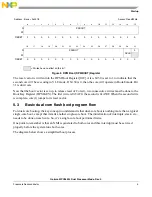
Figure 3. Connecting to MPC5643L

4. Specify the programming algorithm to use. In this case, select the file from the P&E tools 

installation folder 
.

..\pemicro\algorithms\shadow\Freescale_MPC5643L_1x32x4k_Shadow_Blk_Freescale_C9

0FL2_Driver_031.PCP 

to enable program and erase operations on the shadow flash.

6.2

Dump shadow flash to s-record file

After the programming tool has been configured for the MPC5643L shadow flash, the existing contents of 
the shadow flash should be dumped to an s-record file. The file will be used to change the configuration.

1. From the menu bar, select Upload 

 Upload Module.

2. Specify a name for the s-record .s19 file.

6.3

Modify s-record file to change LSM/DPM configuration

The s-record file can now be edited to modify the LSM/DPM configuration. The s-record file format 
S2xxyyyyyyzzzzcs is as follows:

S2
Single-character start code S followed by a single-character record type. S2 indicates the line is a 
data sequence with 3 bytes of address.

xx
Two hexadecimal digits indicating the byte count in hexadecimal (a data + checksum). 

yyyyyy
Six hexadecimal digits to indicate the three bytes of address that specify the memory location of 
the first data byte

zzzz
Zero to sixty-four pairs of hexadecimal characters specifying the data bytes

cs
Two hex digits indicating the checksum, which is calculated by taking the sum of the all the bytes 

Содержание Qorivva MPC5643L

Страница 1: ...The MPC5643L operates in both lock step mode and DPM this paper will focus on the DPM mode 1 Scope 1 2 Reference material 1 3 Overview 1 4 MPC5643L dual core architecture 2 4 1 Block diagram 3 4 2 Sp...

Страница 2: ...on as about 1 6 the performance of the LS mode at the same frequency In the DP mode each CPU core and each connected channel run independently from the other one and redundancy checkers RCCU are disab...

Страница 3: ...ual processor mode these same peripherals have unique addresses On core 0 the SoR peripherals remain at the LSM addresses and the core 1 SoR peripherals are now visible at a different set of addresses...

Страница 4: ...r configuration is located at offset 0x3E10 This is also readable at flash register BIU4 Flash_regs_base 0x2C Refer to Section 6 Changing between LSM and DPM for detailed instructions on how to progra...

Страница 5: ...flow For dual core booting the key concept to understand is that dual core boot is nothing more than a typical single core boot except that it starts another single core boot The initialization of in...

Страница 6: ...0 setting up the start address for core 1 Place Reset Vector for Core 1 in register P2BOOT Release Reset for Core 1 by writing DPMKEY No Core 1 runs MMU setup other initialization including NMI vector...

Страница 7: ...pon return from the NMI both cores are now fully functional and operating independently It is important for the NMI routines to be included because the NMI interrupt is triggered when the system moves...

Страница 8: ...configuration 1 From the menu bar select Upload Upload Module 2 Specify a name for the s record s19 file 6 3 Modify s record file to change LSM DPM configuration The s record file can now be edited to...

Страница 9: ...This change requires the checksum to be recalculated as follows 0xFF 0x14 0xFF 0xFE 0x10 0xFF 0xBF 0xFF 0xFF 0xFF 0xFF 0xFF 0xFF 0xFF 0xFF 0xFF 0xFF 0xFF 0xFF 0xFF 0xFF mod 256 0x2E Example 2 Modifie...

Страница 10: ...cond core requires the same kind of initialization code as used on the first core So the end result is really a single core with peripherals times two There is no additional complexity of code only ad...

Страница 11: ...validated for each customer application by customer s technical experts Freescale does not convey any license under its patent rights nor the rights of others Freescale sells products pursuant to stan...

Отзывы: