


NXP Semiconductors
UM11711
PCAL6524EV-ARD evaluation board
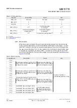
Bus line
Direct Write
Count
Idle
MAX_CLK
Not used
Not used
Not used
MAX_CLR
0
0
1
MAX_OE
0
1
0
MAX_CTRL_0
Controls the speed
of counting
MAX_CTRL_1
Controls the indication
of digit 4 (D9).
Controls the direction
of counting
0
MAX_CTRL_2
X
Controls the counting status
X
Table 3. CPLD control bus
[1]
Don’t care
[2]
See
[3]
See
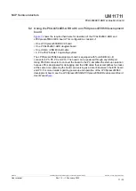
4.9.1 Direct write
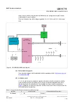
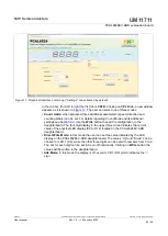
When this mode is activated, the user can write decimal values from the GUI directly
to the on-board LED display on the PCAL6524EV-ARD board. For the Digit 1, 2, and 3
(D10, D11, and D12), the user can write decimal numbers from 0 to 9. For Digit 4 (D9),
the user can set the letter “U” or “d” (the initials of “Up” and “down”). Note that the digit
4 indication is controlled by the MAX_CTRL_1 control line (not through the one of I/O
line of the PCAL6524 IC). The dots of the digits can be set separately. See
and
PCAL6534 pin
Direct write
Count
Idle
P0_0
P0_1
P0_2
P0_3
Write decimal numbers from the GUI to
Digit 1 (D12). The PCAL6524 pins are
configured as outputs.
Read the current data from
Digit 1 (D12). The PCAL6524
pins are configured as inputs.
P0_4
P0_5
P0_6
P0_7
Write decimal numbers from the GUI to
Digit 2 (D11). The PCAL6524 pins are
configured as outputs.
Read the current data from
Digit 2 (D11). The PCAL6524
pins are configured as inputs.
P1_0
P1_1
P1_2
P1_3
Write decimal numbers from the GUI to
Digit 3 (D10). The PCAL6524 pins are
configured as outputs.
Read the current data from
Digit 3 (D10). The PCAL6524
pins are configured as inputs.
P1_4
Set ON/OFF the dot of Digit 1 (D12)
P1_5
Set ON/OFF the dot of Digit 2 (D11)
P1_6
Set ON/OFF the dot of Digit 3 (D10)
P1_7
Set ON/OFF the dot of Digit 4 (D9)
The PCAL6524 pins are
configured as inputs. The
lines are set in high state in
MAX V.
No action. The MAX V
corresponding pins are in high
Z.
Table 4. MAX V data bus
UM11711
All information provided in this document is subject to legal disclaimers.
© NXP B.V. 2022. All rights reserved.
User manual
Rev. 1.0 — 19 January 2022
11 / 30