GENERAL-PURPOSE TIMER
M68HC16 Z SERIES
11-2
USER’S MANUAL
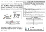
Figure 11-1 GPT Block Diagram
11.2 GPT Registers and Address Map
The GPT programming model consists of a configuration register (GPTMCR), parallel
I/O registers (DDRGP, PORTGP), capture/compare registers (TCNT, TCTL1, TCTL2,
TIC[1:3], TOC[1:4], TI4/O5, CFORC), pulse accumulator registers (PACNT, PACTL),
pulse-width modulation registers (PWMA, PWMB, PWMC, PWMCNT, PWMBUFA,
PWMBUFB), status registers (TFLG1, TFLG2) and interrupt control registers (TMSK1,
TMSK2). Functions of the module configuration register are discussed in
and
11.4 Polled and Interrupt-Driven Operation
. Other regis-
ter functions are discussed in the appropriate sections.
All registers can be accessed using byte or word operations. Certain capture/compare
registers and pulse-width modulation registers must be accessed by word operations
to ensure coherency. If byte accesses are used to read a register such as the timer
counter register (TCNT), there is a possibility that data in the byte not being accessed
will change while the other byte is read. Both bytes must be accessed at the same
time.
The modmap (MM) bit in the system integration module configuration register
(SIMCR) defines the most significant bit (ADDR23) of the IMB address for each regis-
ter in the MCU. Because the CPU16 drives ADDR[23:20] to the same logic state as
ADDR[19:0], MM must equal one.
GPT BLOCK
PULSE ACCUMULATOR
PWM UNIT
BUS INTERFACE
IMB
CAPTURE/COMPARE UNIT
PRESCALER
IC1/PGP0
IC2/PGP1
IC3/PGP2
PCLK
PWMB
PWMA
PAI
IC4/OC5/OC1/PGP7
OC4/OC1/PGP6
OC3/OC1/PGP5
OC2/OC1/PGP4
OC1/PGP3
F
re
e
sc
a
le
S
e
m
ic
o
n
d
u
c
to
r,
I
Freescale Semiconductor, Inc.
For More Information On This Product,
Go to: www.freescale.com
n
c
.
..


