


UM11158
All information provided in this document is subject to legal disclaimers.
© NXP B.V. 2022. All rights reserved.
User manual
Rev. 1.6 — 17 March 2022
21 of 24
NXP Semiconductors
UM11158
LPCXpresso55S69/55S28 Development Boards
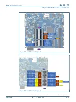
SDIO port 1 of the LPC55Sxx is routed to the expansion connector to provide access to
this interface. Note that the power enable signal used for this SDIO interface is not one of
the port pins that supports in SD1_POWER_EN function; this because all port pins that
support this function are required for other features of the board. PIO1_16 is used instead
for the power enable function, configured as a GPIO.
9. Other
features
This section describes miscellaneous board features that we not covered elsewhere in
this manual.
9.1 LPC55Sxx ADC references and inputs
By default, the LPC55Sxx ADC positive reference is connected to VDDA and the negative
reference to ground. Different reference voltages may be used by moving the zero ohm
link J8 or J9 (for positive or negative reference respectively) from the 1-2 to the 2-3
position, and connecting an external reference to P15 (pin 1 for positive, pin 3 for
negative).
An external differential ADC input signal can be applied at P28 or at the P19 expansion
connector. This connection is routed to PIO0_16 and PIO0_23.
10. Errata
10.1 Brown-out detect (BOD) may be triggered during boot (code
execution from ROM)
Initial production LPCXpresso55S69 boards, marked as Revision A1, use LPC55S69
revision 0A silicon. Please refer to errata documentation from NXP for full details of device
errata (https://www.nxp.com/docs/en/errata/ES_LPC55S6x.pdf).
Revision A2 boards have a 1.8V regulator installed that has a 2% tolerance. This can
result in the supply voltage being below the specification of the LPC55Sxx device and
thus in some cases the brown-out detect (BOD) of the device may trigger during boot
(code execution from ROM). If this occurs it will prevent an application programmed in
SRAM or flash from executing. In this situation an external 1.8V supply may be connected
to the center pin of P4 to power the LPC55Sxx device. Note that board designs should
use a regulator that guarantees a minimum 1.8V supply; alternative regulators with 1.9V
or 2V outputs are available from Torex in their XC6203 family in the same footprint, and
also in the XC6503 range, and other alternatives are available from other suppliers.
Revision A1 and A2 boards have some passive components installed that are not
necessary and should be omitted in application designs; see
.
10.2 SPI ISP
mode
SPI ISP mode is not supported since the pins assigned use Flexcomm 3. SPI ISP mode is
supported only on the High-Speed SPI port pins.