


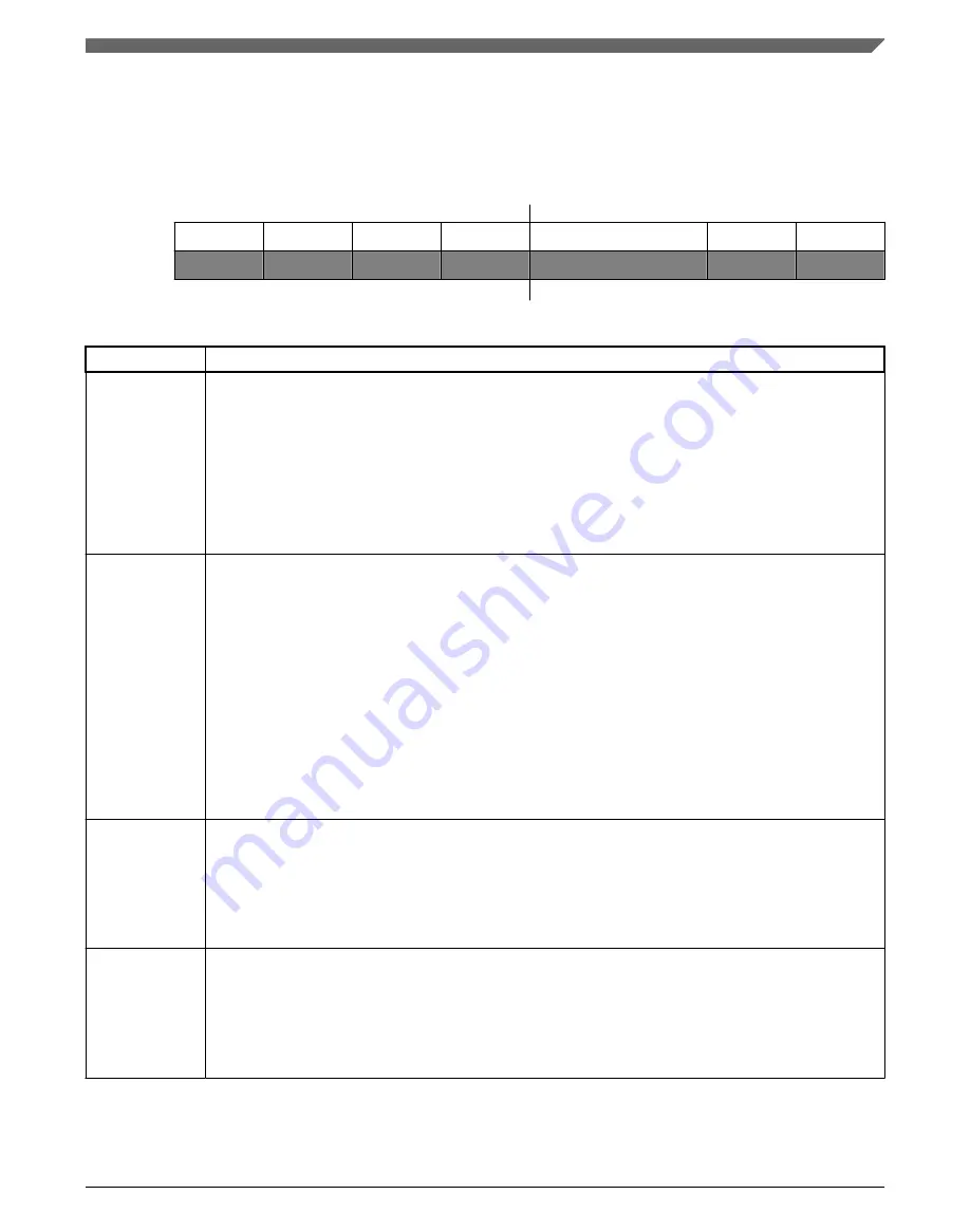
25.3.7 MCG Status Register (MCG_S)
Address: 4006_4000h base + 6h offset = 4006_4006h
Bit
7
6
5
4
3
2
1
0
Read
Write
Reset
0
0
0
1
0
0
0
0
MCG_S field descriptions
Field
Description
7
LOLS0
Loss of Lock Status
This bit is a sticky bit indicating the lock status for the PLL. LOLS is set if after acquiring lock, the PLL
output frequency has fallen outside the lock exit frequency tolerance, D
unl
. LOLIE determines whether an
interrupt request is made when LOLS is set. LOLRE determines whether a reset request is made when
LOLS is set. This bit is cleared by reset or by writing a logic 1 to it when set. Writing a logic 0 to this bit has
no effect.
0
PLL has not lost lock since LOLS 0 was last cleared.
1
PLL has lost lock since LOLS 0 was last cleared.
6
LOCK0
Lock Status
This bit indicates whether the PLL has acquired lock. Lock detection is only enabled when the PLL is
enabled (either through clock mode selection or PLLCLKEN0=1 setting). While the PLL clock is locking to
the desired frequency, the MCG PLL clock (MCGPLLCLK) will be gated off until the LOCK bit gets
asserted. If the lock status bit is set, changing the value of the PRDIV0 [4:0] bits in the C5 register or the
VDIV0[4:0] bits in the C6 register causes the lock status bit to clear and stay cleared until the PLL has
reacquired lock. Loss of PLL reference clock will also cause the LOCK0 bit to clear until the PLL has
reacquired lock. Entry into LLS, VLPS, or regular Stop with PLLSTEN=0 also causes the lock status bit to
clear and stay cleared until the Stop mode is exited and the PLL has reacquired lock. Any time the PLL is
enabled and the LOCK0 bit is cleared, the MCGPLLCLK will be gated off until the LOCK0 bit is asserted
again.
0
PLL is currently unlocked.
1
PLL is currently locked.
5
PLLST
PLL Select Status
This bit indicates the clock source selected by PLLS . The PLLST bit does not update immediately after a
write to the PLLS bit due to internal synchronization between clock domains.
0
Source of PLLS clock is FLL clock.
1
Source of PLLS clock is PLL output clock.
4
IREFST
Internal Reference Status
This bit indicates the current source for the FLL reference clock. The IREFST bit does not update
immediately after a write to the IREFS bit due to internal synchronization between clock domains.
0
Source of FLL reference clock is the external reference clock.
1
Source of FLL reference clock is the internal reference clock.
Table continues on the next page...
Chapter 25 Multipurpose Clock Generator (MCG)
K22F Sub-Family Reference Manual, Rev. 4, 08/2016
NXP Semiconductors
551
Содержание K22F series
Страница 2: ...K22F Sub Family Reference Manual Rev 4 08 2016 2 NXP Semiconductors...
Страница 150: ...Private Peripheral Bus PPB memory map K22F Sub Family Reference Manual Rev 4 08 2016 150 NXP Semiconductors...
Страница 168: ...Module clocks K22F Sub Family Reference Manual Rev 4 08 2016 168 NXP Semiconductors...
Страница 198: ...Security Interactions with other Modules K22F Sub Family Reference Manual Rev 4 08 2016 198 NXP Semiconductors...
Страница 258: ...Functional description K22F Sub Family Reference Manual Rev 4 08 2016 258 NXP Semiconductors...
Страница 292: ...Functional description K22F Sub Family Reference Manual Rev 4 08 2016 292 NXP Semiconductors...
Страница 398: ...Functional description K22F Sub Family Reference Manual Rev 4 08 2016 398 NXP Semiconductors...
Страница 628: ...Initialization and application information K22F Sub Family Reference Manual Rev 4 08 2016 628 NXP Semiconductors...
Страница 740: ...Initialization Application Information K22F Sub Family Reference Manual Rev 4 08 2016 740 NXP Semiconductors...
Страница 750: ...Functional description K22F Sub Family Reference Manual Rev 4 08 2016 750 NXP Semiconductors...
Страница 816: ...Application information K22F Sub Family Reference Manual Rev 4 08 2016 816 NXP Semiconductors...
Страница 866: ...Initialization Application Information K22F Sub Family Reference Manual Rev 4 08 2016 866 NXP Semiconductors...
Страница 890: ...Application information K22F Sub Family Reference Manual Rev 4 08 2016 890 NXP Semiconductors...
Страница 1028: ...Initialization Procedure K22F Sub Family Reference Manual Rev 4 08 2016 1028 NXP Semiconductors...
Страница 1040: ...Example configuration for chained timers K22F Sub Family Reference Manual Rev 4 08 2016 1040 NXP Semiconductors...
Страница 1118: ...Device mode IRC48 operation K22F Sub Family Reference Manual Rev 4 08 2016 1118 NXP Semiconductors...
Страница 1122: ...USB Voltage Regulator Module Signal Descriptions K22F Sub Family Reference Manual Rev 4 08 2016 1122 NXP Semiconductors...
Страница 1180: ...Initialization application information K22F Sub Family Reference Manual Rev 4 08 2016 1180 NXP Semiconductors...
Страница 1302: ...Application information K22F Sub Family Reference Manual Rev 4 08 2016 1302 NXP Semiconductors...
Страница 1374: ...Functional description K22F Sub Family Reference Manual Rev 4 08 2016 1374 NXP Semiconductors...