NXP Semiconductors FRDMGD3160XM3EVM Скачать руководство пользователя страница 35

NXP Semiconductors

UM11620

FRDMGD3160XM3EVM half-bridge evaluation board

Problem

Evaluation

Explanation

Corrective action(s)

Check bit length of message sent

There is SPIERR if SCLK does not

see a n*24 multiple of cycles

Use 24-bit message length for SPI

messages

Check CRC

SPIERR faults if CRC provided in

sent message is not good

Use FlexGUI to generate commands

with valid CRC. The command can be

copied in binary or hexadecimal and

sent from another program.

SPIERR reported after SPI message

Check for sufficient dead time

between SPI messages

SPIERR fault bit is set when the time

between SPI messages (txfer_delay)

received is too short. Minimum

required delay time is 19 µs.

Check time between CSB rising edge

(old message end) and CSB falling

edge (new message start) during

normal SPI read, and ensure transfer

delay dead time check.
SPIERR can also be cleared in BIST.

VCCREGUV reported on startup

Check VCCREG potential

Caused by low VCC

Clear VCCREGUV fault bit

(STATUS1).
Tune VCC-GNDISO potential with

power supply set resistor (R20).

Check HV domain is powered

correctly

Related to slow rise time of VCC

supply on HV domain, or failed VREF

regulator

Clear VREFUV bit (STATUS2).
Reset HV domain supply if fault bit

does not clear.

VREFUV reported on startup

Check VCC for undervoltage

condition

Low VCC is visible indirectly through

other HV domain faults

Tune VCC-GNDISO using R20

feedback

Check VEE level on suspect domain. If VEE level is not at desired negative

voltage it could cause excessive VCC

level.

Check Zener diode in power supply

circuit for proper value in setting VEE

level.
Clear VCCOV bit (STATUS1) to

continue.

VCCOV fault reported on startup

Check VCC-GNDISO potential

PWM is disabled during a VCC

overvoltage (20 V nom.)

Tune VCC-GNDISO potential to

suitable level with power supply set

resistor (R22).
Clear VCCOV bit (STATUS1) to

continue.

No PWM during short circuit test

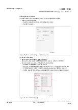
Check PWMALT jumpers

Incorrect configuration of PWMALT

pins prevent short-circuit test by

enforcing dead time

For short-circuit test, set PWMALTL

(J9) and PWMALTH (J10) to bypass

dead time. See 

Section 4.4.3

 for

details.

Check VSUP/VDD for undervoltage

condition

VDD_UV latches SPI buffer contents,

preventing updated fault reporting.

Check voltage provided at VDD pin

(pin 3).
On each read, compare the address

from the sent command and response

(a difference indicates that the SPI

response is latched due to inactive).

Read multiple addresses to ensure a

good comparison.

Check PS_EN is set to HIGH in

FlexGUI; see 

Figure 22

VCC/VEE can be enabled/disabled in

software.

Enable VCC/VEE from FlexGUI

Bad SPI data, appears to repeat

previous response

Check VCC for undervoltage

Unpowered VCC prevents HV domain

from updating data

Tune VCC-GNDISO using R22

feedback

7 Schematics, board layout, and bill of materials

The board schematics, board layout, and bill of materials are available at 

http://

www.nxp.com/FRDMGD3160XM3EVM

 on the Overview tab under Get Started.

8 References

[1] Tool summary page for FRDMGD3160XM3EVM 

http://www.nxp.com/FRDMGD3160XM3EVM

[2] Product summary page for GD3160 device 

http://www.nxp.com/GD3160

UM11620

All information provided in this document is subject to legal disclaimers.

© NXP B.V. 2021. All rights reserved.

User guide

Rev. 1 — 10 June 2021

35 / 38

Содержание FRDMGD3160XM3EVM

Страница 1: ...on board XM3 GD3160 Abstract The FRDMGD3160XM3EVM is a functional power module half bridge kit This kit can be used as a foundation on which to develop and analyze the GD3160 gate driver for ASIL D co...

Страница 2: ...lf bridge evaluation board Revision Date Description 1 20210610 initial version Revision history UM11620 All information provided in this document is subject to legal disclaimers NXP B V 2021 All righ...

Страница 3: ...dependent on proper printed circuit board layout and heat sinking design as well as attention to supply filtering transient suppression and I O signal quality The goods provided may not be complete in...

Страница 4: ...160XM3EVM half bridge evaluation board 2 FRDMGD3160XM3EVM Figure 1 FRDMGD3160XM3EVM UM11620 All information provided in this document is subject to legal disclaimers NXP B V 2021 All rights reserved U...

Страница 5: ...the FRDMGD3160XM3EVM 1 Go to http www nxp com FRDMGD3160XM3EVM 2 On the Overview tab locate the Jump To navigation feature on the left side of the window 3 Select the Get Started link review each ent...

Страница 6: ...al interface SPI registers on the GD3160 gate drive devices in either daisy chain or standalone configuration The KITGD3160TREVB translator board is used to translate 3 3 V signals to 5 0 V signals be...

Страница 7: ...and sink Interrupt pin for fast response to faults Compatible with negative gate supply Compatible with 200 V to 1700 V IGBT and SiC MOSFET power range 125 kW Table 1 Device features 4 4 Board descrip...

Страница 8: ...omain is 15 V VSUP domain that interfaces with the MCU and GD3160 control registers through the 24 pin connector interface Low side driver and high side driver domains are driver control interfaces to...

Страница 9: ...modulation PWM input low side 6 INTBL interrupt bar low side 7 MOSIL master out slave in low side 8 SCLK serial clock input 9 MISOL master in slave out low side 10 EN_PS MCU control of flyback power...

Страница 10: ...nd low side 20 AOUTH duty cycle encoded signal high side 21 PWMH PWM input high side 22 FSSTATEH fail safe state high side 23 GND ground 24 INTBH interrupt bar high side Table 2 Low voltage domain 24...

Страница 11: ...test point VEEL negative voltage supply test point for low side driver gate of IGBT or SiC module CLMPL active clamping low side test point VDC DC link voltage test point at voltage divider COLL coll...

Страница 12: ...t testing open VCCREG controls gate voltage VCCH and VCCL R25 and R46 closed VCC and VCCREG are tied together open internally regulated supply derived from VSUP VDDH and VDDL R28 and R47 closed VSUP V...

Страница 13: ...ion socket Description NTC NTC connection to module for monitoring temperature V high side drain connection G1 high side gate connection G2 low side gate connection Table 5 Power module connections UM...

Страница 14: ...gate low resistor in series with the GL pin at the output of the GD3160 gate low driver and XM3 module gate that controls the turn off current for SiC MOSFET gate RAMC series resistor between XM3 modu...

Страница 15: ...icating reported fault status when on active LOW High side INTB connected to the INTB interrupt output pin of high side driver indicating reported fault status when on active LOW Low voltage power ind...

Страница 16: ...he Freedom KL25Z is an ultra low cost development platform for Kinetis L series MCU built on Arm Cortex M0 processor Figure 9 Freedom development platform UM11620 All information provided in this docu...

Страница 17: ...e VCCSEL J3 2 3 selects 3 3 V for 3 3 V compatible gate drive 1 2 selects PWM high side control from KL25Z MCU PWMH_SEL J4 2 3 selects PWM high side control from fiber optic receiver inputs 1 2 select...

Страница 18: ...ple rate digital oscilloscope with probes DC link capacitor compatible with XM3 module IGBT or SiC MOSFET XM3 module Windows based PC High voltage DC power supply for DC link voltage Low voltage DC po...

Страница 19: ...tall this software as a backup or to help debugging 6 1 Installing FlexGUI on your computer The latest version of FlexGUI supports the GD3100 and GD3160 It is designed to run on any Windows 10 or Wind...

Страница 20: ...1 To clear the memory and place the board in boot loader mode hold down the reset button while plugging a USB cable into the OpenSDA USB port 2 Verify that the board appears as a BOOTLOADER device an...

Страница 21: ...data associated with a single unplug event 6 3 Using the FlexGUI The FlexGUI is available from http www nxp com FlexGUI as an evaluation tool demonstrating GD31xx specific functionality configuration...

Страница 22: ...gure 14 Kit selection FlexGUI settings Access settings by selecting Settings from the File menu Figure 15 GUI settings menu UM11620 All information provided in this document is subject to legal discla...

Страница 23: ...luation board The Loader and Logs settings are shown below Figure 16 Loader settings Figure 17 Logs settings UM11620 All information provided in this document is subject to legal disclaimers NXP B V 2...

Страница 24: ...lecting Settings from the File menu The Register Map and Tabs settings are shown below Figure 18 Register map settings Figure 19 Tabs settings UM11620 All information provided in this document is subj...

Страница 25: ...board Command Log window The Command Log area informs the user about application events Figure 20 Command Log area UM11620 All information provided in this document is subject to legal disclaimers NX...

Страница 26: ...hown Read and automatically poll INTB pins INTA pins are added for GD3160 Control pins set values to a default to a functional state FSENB enable disable fail safe enable EN_PS enables flyback supply...

Страница 27: ...r all faults and automatically poll status registers Figure 23 Status tab functionality Analog tab functionality Read and poll ADC values from the high voltage domain Displays raw ADC and converted va...

Страница 28: ...using the W button Copy button to copy the read values to the write line can be set to copy automatically Reset button to undo the changes on the write line and reset to the previous value Global regi...

Страница 29: ...All settings are automatically synchronized with the register controls Figure 26 Gate drive tab Current Sense tab Allows setting of parameters related to current sense Provides a more intuitive visual...

Страница 30: ...lated to desat and segmented drive Provides a more intuitive visual way to set parameters All settings are automatically synchronized with the register controls Figure 28 Desat and segmented drive tab...

Страница 31: ...chronized with the register controls Figure 29 Overtemperature tab Undervoltage threshold tab Allows setting of parameters related to undervoltage threshold Provides a more intuitive visual way to set...

Страница 32: ...on board Measurements tab Allows monitoring and graphing of ADC and temperature values Figure 31 Measurements tab UM11620 All information provided in this document is subject to legal disclaimers NXP...

Страница 33: ...mask registers can be modified when in configuration mode Figure 32 Status tab Pulse tab Used for double pulse short circuit and PWM testing Select desired T1 T2 and T3 timings for each test type sel...

Страница 34: ...ister Dead time is enforced but fault indicates that PWM controls signals are in violation Clear DTFLT fault bit STATUS2 Check PWMALTL J9 and PWMALTH J10 are configured to bypass dead time faults Cons...

Страница 35: ...er diode in power supply circuit for proper value in setting VEE level Clear VCCOV bit STATUS1 to continue VCCOV fault reported on startup Check VCC GNDISO potential PWM is disabled during a VCC overv...

Страница 36: ...customer s third party customer s NXP does not accept any liability in this respect Terms and conditions of commercial sale NXP Semiconductors products are sold subject to the general terms and condit...

Страница 37: ...elopment platform 16 Fig 10 Translator board 17 Fig 11 Evaluation board and system setup 18 Fig 12 XM3 module dimensions 19 Fig 13 FRDM KL25Z setup and interface 20 Fig 14 Kit selection 22 Fig 15 GUI...

Страница 38: ...cators 15 4 5 Kinetis KL25Z Freedom board 16 4 6 3 3 V to 5 0 V translator board 17 5 Configuring the hardware 18 6 Installation and use of software tools 19 6 1 Installing FlexGUI on your computer 19...

Отзывы: