Hardware description
Figure 23: NFC input schematic
4397_497 v1.2
26
Страница 1: ...nRF52 Preview Development Kit User Guide v1 2 4397_497 v1 2 2017 02 15 ...
Страница 2: ...rface MCU firmware FW 10 5 4 MSD 10 6 Hardware description 12 6 1 Hardware drawings 12 6 2 Block diagram 13 6 3 Power supply 13 6 4 Connector interface 15 6 5 Buttons and LEDs 17 6 5 1 I O expander for buttons and LEDs 18 6 6 32 768 kHz crystal 20 6 7 Measuring current 21 6 8 RF measurements 22 6 9 Debug input 23 6 10 Debug output 24 6 11 NFC antenna interface 25 Legal notices 27 4397_497 v1 2 ii ...
Страница 3: ...Revision history Date Version Description February 2017 1 2 Created PDF Added MSD on page 10 Updated Interface MCU firmware FW on page 10 4397_497 v1 2 iii ...
Страница 4: ...lution Buttons and LEDs for user interaction I O interface for Arduino form factor plug in modules SEGGER J Link OB Debugger with debug out functionality Virtual COM Port interface via UART Drag and drop Mass Storage Device MSD programming Supporting NFC A listen mode For access to firmware source code hardware schematics and layout files see www nordicsemi com Figure 1 1 nRF52 Preview Development...
Страница 5: ...Introduction 4397_497 v1 2 5 ...
Страница 6: ...nstall nRFgo Studio which includes the nRF Tools package JLinkARM JLink CDC nRFjprog and mergehex from nRFgo Studio b Keil MDK ARM Download and install the latest Keil MDK ARM from Keil MDK ARM Development Kit c nRF5 SDK Download and extract the latest nRF5 SDK found on developer nordicsemi com d Keil Device Family Pack Install the Device Family Pack that is shipped with the SDK or let Keil instal...
Страница 7: ...d 4 3 or later nRF Master Control Panel for Android 4 3 or later is a powerful generic tool that allows you to scan and explore your Bluetooth Smart devices and communicate with them on an Android phone MCP supports a number of Bluetooth SIG adopted profiles together with the Device Firmware Update DFU profile from Nordic Semiconductor S132 SoftDevice Bluetooth Smart concurrent multi link protocol...
Страница 8: ...led example without having to use the full toolchain it is a matter of copying and pasting a precompiled hex file onto your development kit board Compiling and running a first example Test that you have set up your toolchain correctly by compiling programming and running a very simple example Running examples that use a SoftDevice Before you can run more advanced examples that use Bluetooth or ANT...
Страница 9: ... used to enter the bootloader mode of the Interface MCU To enter bootloader mode keep the reset button pressed while powering up the board until LED LD5 starts to blink You can power up the board either by disconnecting and reconnecting the USB cable or toggle the power switch SW6 Important Pin reset can be enabled by defining the CONFIG_GPIO_AS_PINRESET variable in the project settings This can b...
Страница 10: ...ader This makes it possible to update the SEGGER J Link OB interface firmware For more information on entering the bootloader mode see IF Boot Reset button on page 9 To update Interface MCU firmware drag the Interface image bin into the mounted bootloader drive on the connected computer and power cycle the board It is also possible to download the latest SEGGER J Link software from SEGGER J Link S...
Страница 11: ...and quarantines the unit If this happens the interface MCU will become unresponsive If the computer is set up to boot from USB it can try to boot from the development kit if the development kit is connected during boot This could be avoided by unplugging the development kit before a computer restart or changing the boot sequence of the computer You can also disable the MSD of the kit by using the ...
Страница 12: ...lution In addition to radio communication the nRF52832 device can communicate with a computer through a virtual COM port provided by the interface MCU 6 1 Hardware drawings nRF52 Preview Development Kit hardware drawings show both sides of the PCA10036 board Figure 3 nRF52 Preview Development Kit board top view Figure 4 nRF52 Preview Development Kit board bottom view 4397_497 v1 2 12 ...
Страница 13: ...Interface MCU VBUS USB sense Data Osc 32 768 kHz IF Boot Reset UART SWD VCC_nRF Osc 32 MHz Debug in Debug out Power switch Power switch Matching network NFC antenna SWF switch RF connector I O expander Debouncing filter Switch Switch Figure 5 nRF52 Preview Development Kit board block diagram 6 3 Power supply The nRF52 Preview Development Kit board has three power options 5 V from the USB external ...
Страница 14: ...hest voltage Important When USB is not powered the Interface MCU is in dormant state and will draw an additional current of 20 μA in order to maintain the reset button functionality This will affect board current consumption but not the nRF52832 current measurements as described in Measuring current on page 21 Figure 7 Power supply circuitry The reverse voltage protection diodes will add a voltage...
Страница 15: ...ridges Figure 8 Protection diode bypass solder bridges Important Connect only one power source at the time Shorting the solder bridges removes the reverse voltage protection 6 4 Connector interface Access to the nRF52832 GPIOs is available from connectors P2 P3 P4 P5 and P6 The P1 connector provides access to ground and power on the nRF52 Preview Development Kit board 4397_497 v1 2 15 ...
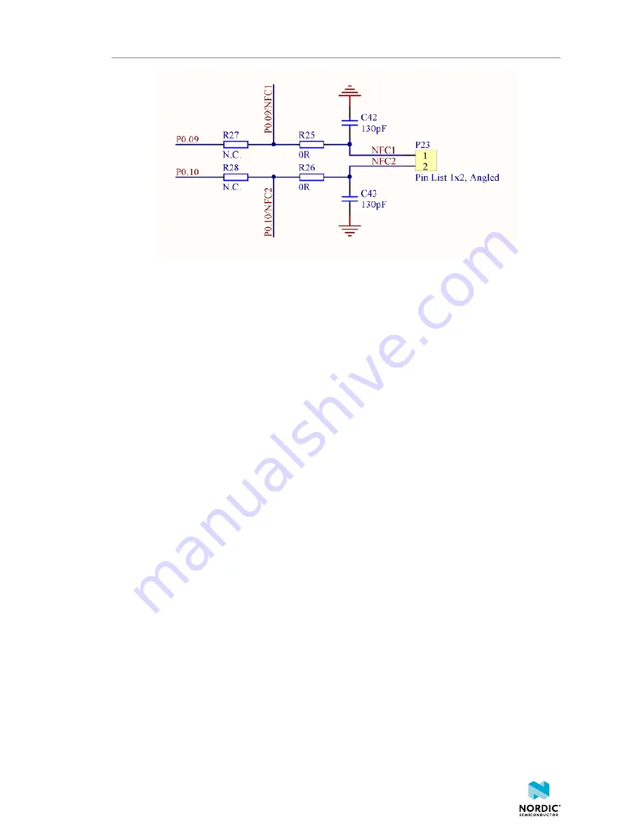
Страница 16: ...he 32 kHz crystal and are not available on the connectors For more information see Section 32 768 kHz crystal on page 20 P0 05 P0 06 P0 07 and P0 08 are by default used by the UART connected to the Interface MCU For more information see Section Virtual COM port on page 9 P0 09 and P0 10 are by default used by NFC1 and NFC2 For more information see Section NFC antenna interface on page 25 P0 13 P0 ...
Страница 17: ...rt Button 1 P0 13 Button 2 P0 14 Button 3 P0 15 Button 4 P0 16 LED 1 P0 17 SB5 LED 2 P0 18 SB6 LED 3 P0 19 SB7 LED 4 P0 20 SB8 Table 3 Button and LED connection If GPIO P0 17 P0 20 are needed elsewhere the LEDs can be disconnected by cutting the short on SB5 SB8 see Figure 11 Disconnecting the LEDs on page 18 The LEDs and buttons can also be disconnected by using the I O extender as described in I...
Страница 18: ... as an input with an internal pull up resistor The LEDs are active low meaning that writing a logical zero 0 to the output pin will illuminate the LED Figure 12 Button and LED configuration 6 5 1 I O expander for buttons and LEDs The nRF52 Preview Development Kit board has an I O expander to avoid conflicts with boards that follow the Arduino standard the on board GPIOs for the buttons and LEDs wo...
Страница 19: ... The I O expander can be permanently enabled by shorting solder bridge SB18 or permanently disabled by cutting the shorting track on SB19 You must also short SB18 when cutting SB19 for full compatibility with the Arduino standard The I O extender can be temporarily enabled by connecting SHIELD DETECT to ground Figure 13 Enable or disable I Os for Arduino standard In addition to the buttons and LED...
Страница 20: ...n the nRF52 Preview Development Kit board P0 00 and P0 01 are by default used for the 32 768 kHz crystal and are not available as a GPIO on the connectors Important When using ANT ANT the 32 768 kHz crystal X2 is required for correct operation If P0 00 and P0 01 are needed as normal I Os the 32 768 kHz crystal can be disconnected and the GPIO routed to the connectors Cut the shorting track on SB1 ...
Страница 21: ...pere meter or an oscilloscope 1 Ampere meter a Connect an ampere meter between the pins of connector P22 This will monitor the current directly Figure 17 Current measurement with ampere meter 2 Oscilloscope a Mount a resistor on the footprint for R6 The resistor should not be larger than 10 Ω b Connect an oscilloscope in differential mode or similar with two probes on the pins of the P22 connector...
Страница 22: ...of the RF signal The connector is of SWF type from Murata part no MM8130 2600 with an internal switch By default when there is no cable attached the RF signal is routed to the on board PCB trace antenna A test probe is available from Murata part no MXHS83QE3000 with a standard SMA connection on the other end for connecting instruments When connecting the test probe the internal switch in the SWF c...
Страница 23: ... when doing measurements see Table 6 Typical loss in connector and test probe on page 23 Frequency MHz Loss dB 2440 1 0 4880 1 7 7320 2 6 Table 6 Typical loss in connector and test probe 6 9 Debug input The Debug in connector P18 makes it possible to connect external debuggers for debugging while running on battery or external power supply 4397_497 v1 2 23 ...
Страница 24: ...e supply voltage of the board and program debug the target chip on the external board instead of the on board nRF52832 Important The voltage supported by external debugging programming is 3 0 V You can also use P20 as a debug out connection to program shield mounted targets For the Debug out header P19 the Interface MCU will detect the supply voltage on the mounted shield and program debug the shi...
Страница 25: ...ns and their protection level against abnormal voltages The content of the NFCPINS register is reloaded at every reset Important The NFC pins are enabled by default NFC can be disabled and GPIOs enabled by defining the CONFIG_NFCT_PINS_AS_GPIOS variable in the project settings This can be done by defining the preprocessor symbol in Keil go to Project Options for Target C C Preprocessor Symbols Def...
Страница 26: ...Hardware description Figure 23 NFC input schematic 4397_497 v1 2 26 ...
Страница 27: ...ucts are not designed for use in life support appliances devices or systems where malfunction of these products can reasonably be expected to result in personal injury Nordic Semiconductor ASA customers using or selling these products for use in such applications do so at their own risk and agree to fully indemnify Nordic Semiconductor ASA for any damages resulting from such improper use or sale R...