background image

© National Instruments

|

A-3

NI-793xR User Manual

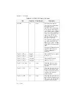
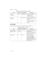
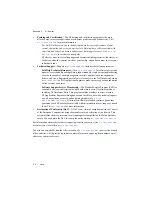
Port<0..1>_Tx_
Disable

Out

Async

When high, this output shuts 
down the transmitter optical 
transmitter. When low, 
operation is enabled.

Port<0..1>_Rs<0..1> 

Out

Async

Rate selection pins.

Port<0..1>_SCL

In/Out

Async

Bidirectional serial clock signal 
for the two-wire communication 
interface on the Port <0..1> 
connector.

Valid values: 

0

 and 

Z

 (open 

drain).

This signal is also called 
MODDEF1.

Port<0..1>_SDA

In/Out

Async

Bidirectional serial data signal 
for the two-wire communication 
interface on the Port <0..1> 
connector.

Valid values: 

0

 and 

Z

 (open 

drain).

This signal is also called 
MODDEF2.

Port<0..1>_
MacAddress

In

Async

Unique 48-bit MAC address 
assigned to Port<0..1>. Use this 
address when implementing a 
network interface controller on 
Port<0..1>.

Port<0..1>_
MacAddressValid

In

Async

When asserted, this signal 
indicates that 
Port<0..1>_MacAddress is 
valid.

Table A-1.  

NI-7932R CLIP Signals (Continued)

Port

Direction

Clock Domain

Description

Содержание 7931R

Страница 1: ...FlexRIO TM NI 7931R 7932R 7935R User Manual NI 793xR User Manual August 2015 375181B 01...

Страница 2: ...ers email addresses and current events National Instruments Corporate Headquarters 11500 North Mopac Expressway Austin Texas 78759 3504 USA Tel 512 683 0100 For further support information refer to th...

Страница 3: ...ESS FOR A PARTICULAR PURPOSE TITLE OR NON INFRINGEMENT AND ANY WARRANTIES THAT MAY ARISE FROM USAGE OF TRADE OR COURSE OF DEALING NI DOES NOT WARRANT GUARANTEE OR MAKE ANY REPRESENTATIONS REGARDING TH...

Страница 4: ...es independent from National Instruments and have no agency partnership or joint venture relationship with National Instruments Patents For patents covering National Instruments products technology re...

Страница 5: ...e encouraged to try to correct the interference by one or more of the following measures Reorient the antenna of the receiver the device suffering interference Relocate the transmitter the device gene...

Страница 6: ...5 NI 7932R 3 6 NI 7932R Key Features 3 9 Clocking Architecture 3 11 NI 7935R 3 12 NI 7935R Key Features 3 15 Clocking Architecture 3 16 Chapter 4 Developing with LabVIEW FPGA Developing with LabVIEW F...

Страница 7: ...Core 5 7 Constraints and Hierarchy 5 8 Documenting Your IP 5 9 Adding MGT Socketed CLIP to the LabVIEW Project 5 9 Configuring MGT Socketed CLIP in the NI 793xR LabVIEW FPGA Targets 5 10 Using Existin...

Страница 8: ...NI 793xR User Manual National Instruments ix Appendix A CLIP Signals Appendix B Using the Fan Appendix C NI Services Glossary...

Страница 9: ...guide for your controller for FlexRIO Available from the Start menu Start All Programs National Instruments NI FlexRIO and at ni com manuals Contains information about installing configuring and trou...

Страница 10: ...ll Programs National Instruments LabVIEW 201x LabVIEW 201x Help or by searching for Real Time Module Help at ni com manuals Browse to the Real Time Module book in the Contents tab for information abou...

Страница 11: ...t DC and AC Switching Characteristics DS182 Contains the DC and AC switching characteristic specifications for the Kintex 7 FPGAs Vivado Design Suite Release Notes Installation and Licensing UG973 Pro...

Страница 12: ...s DOC 15799 The FlexRIO Instrument Development Library is a set of host and FPGA code that provides FPGA capabilities commonly found in instruments such as acquisition engines DRAM interfaces and trig...

Страница 13: ...fundamentals required for NI 793xR development Table 1 1 Fundamentals Resources Concept Resources Real time programming Real time programming courses are available at ni com training You can also ref...

Страница 14: ...m Chapter 1 Before You Begin Xilinx Licensing Information Refer to the Xilinx Documentation section of About This Manual for a list of Xilinx documentation that contains important Xilinx licensing inf...

Страница 15: ...er Caution The NI 793xR mounting orientation is not restricted however when mounting the NI 793xR upside down ensure that the FlexRIO adapter module is supported if you expect shock greater than 30 g...

Страница 16: ...Before using any of these mounting methods record the serial number from the back of the device You will be unable to read the serial number from the back of the device after you have mounted it Caut...

Страница 17: ...e following items to mount the device directly on a flat surface Three screws M4 7 mm thickness of mounting surface Complete the following steps to mount the device 1 Use the dimensions shown in Figur...

Страница 18: ...th optional rubber feet Install the rubber feet to the bottom of the device as shown in Figure 2 3 Caution Do not install rubber feet when directly mounting the NI 793xR The rubber feet will prevent f...

Страница 19: ...ont panel connectors refer to your device s specifications document and the FlexRIO Help For information about connecting the device to a host computer refer to the NI 7931R Getting Started Guide Figu...

Страница 20: ...3 2 ni com Chapter 3 Hardware Architecture The following figure shows the NI 7931R LEDs in more detail Figure 3 2 NI 7931R LEDs RT User LED Power LED Status LED FPGA User LED...

Страница 21: ..._34_n GPIO_34 GND GPIO_35_n GPIO_35 GND GPIO_36_n GPIO_36 GND GPIO_37_n GPIO_37 GND GND PCB Secondary Side Bank 0 PCB Primary Side GND GPIO_CC_14_n GPIO_CC_14 GND GPIO_15_n GPIO_15 GND GPIO_16_n GPIO_...

Страница 22: ...ocessor to USB external storage data transfer rates of 60 MB s Real Time processor to SD external storage data transfer rates of 12 0 MB s read 9 0 MB s write The following figure illustrates the key...

Страница 23: ...locks with LabVIEW FPGA The NI 7931R clocking architecture includes the following clocks 10 MHz Reference Clock 40 MHz Onboard Clock default 100 MHz Clock 200 MHz Clock DRAM Clock The following figure...

Страница 24: ...require calibration The following figure shows the NI 7932R front panel connectors For more information about the front panel connectors refer to your device s specifications document and the FlexRIO...

Страница 25: ...National Instruments 3 7 NI 793xR User Manual The following figure shows the NI 7932R LEDs in more detail Figure 3 7 NI 7932R LEDs RT User LED Power LED Status LED FPGA User LED...

Страница 26: ...4_n GPIO_34 GND GPIO_35_n GPIO_35 GND GPIO_36_n GPIO_36 GND GPIO_37_n GPIO_37 GND GND PCB Secondary Side Bank 0 PCB Primary Side GND GPIO_CC_14_n GPIO_CC_14 GND GPIO_15_n GPIO_15 GND GPIO_16_n GPIO_16...

Страница 27: ...s of 3 125 Gbps 6 25 Gbps and 10 3125 Gbps Kintex 7 XC7K325T FPGA 2 GB onboard FPGA accessible DRAM NI Linux Real Time 32 bit controller FPGA to host data transfer rates of 200 MB s single direction 1...

Страница 28: ...32R Architecture Key Components RT Host RT Controller RAM NV Storage RT Clock Watch Dog LabVIEW Host VI Interrupts DMA Controls Indicators NI Defined Bus Interfaces Streaming IP Memory Controller DRAM...

Страница 29: ...cks 10 MHz Reference Clock 40 MHz Onboard Clock default 100 MHz Clock 156 25 MHz Clock 312 5 MHz MGT Clock1 200 MHz Clock DRAM Clock The following figure illustrates the clocking circuitry on the NI 7...

Страница 30: ...equire calibration The following figure shows the NI 7935R front panel connectors For more information about the front panel connectors refer to your device s specifications document and the FlexRIO H...

Страница 31: ...National Instruments 3 13 NI 793xR User Manual The following figure shows the NI 7935R LEDs in more detail Figure 3 12 NI 7935R LEDs RT User LED Power LED Status LED FPGA User LED...

Страница 32: ...34_n GPIO_34 GND GPIO_35_n GPIO_35 GND GPIO_36_n GPIO_36 GND GPIO_37_n GPIO_37 GND GND PCB Secondary Side Bank 0 PCB Primary Side GND GPIO_CC_14_n GPIO_CC_14 GND GPIO_15_n GPIO_15 GND GPIO_16_n GPIO_1...

Страница 33: ...bidirectional Real Time processor to USB external storage data transfer rates of 60 MB s Real Time processor to SD external storage data transfer rates of 12 0 MB s read 9 0 MB s write The following f...

Страница 34: ...IO system Refer to Chapter 4 Developing with LabVIEW FPGA for information about configuring clocks with LabVIEW FPGA The NI 7935R clocking architecture includes the following clocks 10 MHz Reference C...

Страница 35: ...on the NI 7935R Figure 3 15 NI 7935R Clocking Diagram Memory Controller PLL 40 MHz 100 MHz 100 MHz 10 MHz Reference Clock Kintex 7 FPGA 200 MHz DRAM Clock 166 MHz MGT Oscillator MGT Ref Clk 156 25 MH...

Страница 36: ...uide for your NI 793xR device Adding the NI 793xR to a LabVIEW Project 1 Launch LabVIEW The LabVIEW Getting Started window appears 2 Click Create Project or open an existing project 3 Right click the...

Страница 37: ...e You also can drag and drop existing items into the FPGA target in the Project Explorer window Adding NI 793xR Target I O Complete the following steps to add target I O for the NI 793xR and to access...

Страница 38: ...ou can use the system configuration API to programmatically set the bitfile that is auto loaded on power up Interactive Front Panel Communication Use interactive front panel communication to communica...

Страница 39: ...communication network in LabVIEW FPGA Standard communication methods such as using controls and indicators to pass information between the host and the FPGA may not scale well for large applications U...

Страница 40: ...ry also adds support for arbitration between the read and write ports of DRAM Compiling LabVIEW FPGA VIs You may need to purchase and install additional licenses to compile FPGA designs that incorpora...

Страница 41: ...ecause the FlexRIO adapter module can generate far more data than the application nodes can process The FPGA to Host FIFO uses Ready for Input signals to communicate to the DRAM whether it is ready to...

Страница 42: ...tions in the readiness of the host memory However sizing the FIFO larger consumes block RAM resources on the FPGA and increases the timing pressure on the FIFO NI recommends making the FIFO as large a...

Страница 43: ...ar in your VI Complete the following steps to change the application instance for your simulated FPGA VI 1 Navigate to the bottom left corner of the front panel window or block diagram The application...

Страница 44: ...opment Process If the sample project code is sufficient for your application you do not have to modify the IP core update the VHDL CLIP wrapper or refresh the CLIP Update VHDL CLIP Wrapper Modify rege...

Страница 45: ...itry external to the FPGA Allows your IP to communicate directly with both the FPGA VI and the external adapter module connector interface Socketed CLIP Architecture Figure 5 2 shows an overview of th...

Страница 46: ...NIFPGA programs Vivado2013_4 3 Run the Xilinx Vivado batch file XilinxVivadoDir bin vivado bat You may receive the following warning when launching Vivado Your XILINX_EDK environment variable is unde...

Страница 47: ...urora sample projects for an example of how to use the LabVIEW FPGA AXI4 Lite adapters to connect to DRP within the CLIP Modifying Third Party IP Core Logic If you modify a third party IP core for you...

Страница 48: ...ow to generate an EDIF netlist from the IP core 1 Open the example project for your IP core in Vivado 2 Set the appropriate top level source file for which you plan to generate a netlist 3 Run synthes...

Страница 49: ...or example to create an edf for clock_module_i enter the following command write_edif cell clock_module_i aurora_64b66b_clock_module edf Note You may have to specify a longer path name depending on th...

Страница 50: ...you expose an AXI4 Lite endpoint use Xilinx AXI4 interconnect IP to expose only one AXI4 Lite endpoint to the LabVIEW FPGA diagram Document the frequency of clocks coming from CLIP Consider supportin...

Страница 51: ...need to specify the location of the component within the overall VHDL hierarchy In such cases consider prefacing the constraints with the following macros Prefacing allows the constraints to be appli...

Страница 52: ...ribing which signals are used which signals are unused and the manner in which the signal is used Signal use can affect which ports are active with your IP and the behavior of cables upon ingestion an...

Страница 53: ...LIP using the dialog box or you can click on the Create File icon to create a new CLIP using the CLIP Wizard Note You can modify a CLIP by selecting the preexisting CLIP Declaration Name and clicking...

Страница 54: ...lank 12 Click OK Refer to Chapter 3 Hardware Architecture for more information about NI 793xR clocking capabilities Using Existing VHDL IP inside CLIP or IPIN To use existing IP in your project refer...

Страница 55: ...rations within a given time limit Maximizing determinism is often a priority when designing real time applications Jitter The time difference between the fastest and slowest executions of the applicat...

Страница 56: ...cts like a fixed size queue where the first value you write to the FIFO queue is the first value that you can read from the FIFO queue An RT FIFO ensures deterministic behavior by imposing a size rest...

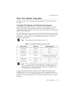
Страница 57: ...ch component s operating range Note All temperatures are reported in degrees Celsius C Note CPU Temp 1 and FPGA Temp are both on die temperature sensors for their respective component CPU Temp 2 and C...

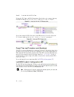
Страница 58: ...work Additionally a device status message appears in MAX under the FPGA item that has been shut down If the FPGA communication shuts down power cycle the system and contact NI customer support at ni...

Страница 59: ...the same VI LabVIEW on the host computer displays the front panel of the VI while the RT Engine executes the block diagram A user interface thread handles the communication between LabVIEW and the RT...

Страница 60: ...g with the front panels of RT target VIs refer to the Interacting with the Front Panels of RT Target VIs topic in the LabVIEW Real Time Module Help Note The Interacting with the Front Panels of RT Tar...

Страница 61: ...to the Real Time Module LabVIEW Real Time Module Release and Upgrade Notes The LabVIEW Real Time Module Release and Upgrade Notes contains information to help you install and configure the Real Time M...

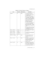
Страница 62: ...P Signals Port Direction Clock Domain Description MGT_RefClk0_p In pad Differential input clock that you must connect to an IBUFDS_GTE2 input buffer primitive when this input clock is used in your des...

Страница 63: ...rom the LabVIEW FPGA VI in the CLIP until aResetS1 is deasserted Port 0 1 _RX_p In pad Dedicated MGT receive signals for Port 0 1 Port 0 1 _RX_n In pad Port 0 1 _TX_p Out pad Dedicated MGT transmit si...

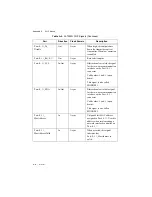
Страница 64: ...drain This signal is also called MODDEF1 Port 0 1 _SDA In Out Async Bidirectional serial data signal for the two wire communication interface on the Port 0 1 connector Valid values 0 and Z open drain...

Страница 65: ...an over power condition is detected Table A 2 NI 7935R CLIP Signals Port Direction Clock Domain Description MGT_RefClk0_p In pad Differential input clock that you must connect to an IBUFDS_GTE2 input...

Страница 66: ...puts from the LabVIEW FPGA VI in the CLIP until aResetS1 is deasserted Port 0 1 _RX_p In pad Dedicated MGT receive signals for Port 0 1 Port 0 1 _RX_n In pad Port 0 1 _TX_p Out pad Dedicated MGT trans...

Страница 67: ...This signal is also called MODDEF1 Port 0 1 _SDA In Out Async Bidirectional serial data signal for the two wire communication interface on the Port 0 1 connector Valid values 0 and Z open drain This s...

Страница 68: ...the power supply to Port 0 1 This signal is active high sPort 0 1 _ PowerGood In SocketClk40 Indicates that the power supply to the cable for Port 0 1 is enabled This signal may deassert if an over po...

Страница 69: ...e NI 793xR includes a replaceable fan assembly For fan troubleshooting information and to order replacement parts refer to ni com support Table B 1 NI 793xR Fan Specifications Manufacturer Sanyo Denki...

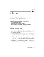
Страница 70: ...you identify your systems accuracy and reliability requirements and provides warranty sparing and calibration services to help you maintain accuracy and minimize downtime over the life of your system...

Страница 71: ...tions Engineers make sure every question submitted online receives an answer Software Support Service Membership The Standard Service Program SSP is a renewable one year subscription included with alm...

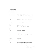
Страница 72: ...communication mechanism used to read and write DRAM DRAM Dynamic random access memory F FPGA Field programmable gate array NI 793xR modules use Xilinx Kintex 7 FPGAs G GPIO General purpose input outpu...

Страница 73: ...Glossary G 2 ni com P PFI Programmable function interface S SCTL Single cycle timed loop SFP Enhanced small form factor pluggable V VHDL VHSIC Hardware Description Language...

Отзывы: