N58 Hardware User Guide
Chapter 5 Application Interfaces
Copyright © Neoway Technology Co., Ltd. All rights reserved.
68
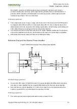
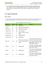
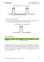
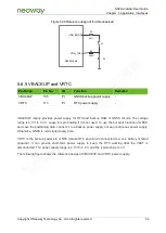
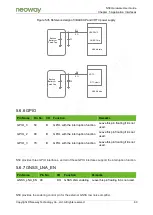
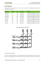
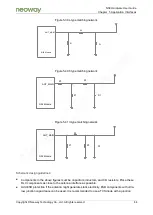
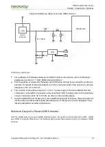
Figure 5-45 Reference design of a passive GNSS antenna
Z1
Z2
Z3
SMA
SAW
Z4
Z5
Z6
LNA
N58 Module
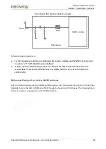
PCB design guidelines:
For guidelines of PCB design between the GNSS interface and antenna, refer to PCB design
guidelines in section 5.7.1 "ANT_MAIN Antenna Interface."
Keep the GNSS RF part far away from the main/BT antenna part. Otherwise, these two parts will
interfere with each other, affecting the RF performance. If the layout is not well designed, it may
interfere with GNSS and affect performance.
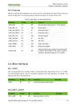
5.7.3 ANT_BT Interface
The 94th pin of the N58 module is a Bluetooth antenna interface pin. It has a characteristic impedance
of 50 Ω.
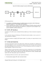
For the schematic design and PCB design of the Bluetooth antenna interface, refer to section 5.7.1
The ANT_BT interface is shared by Wi-Fi signal reception. This interface can support both Wi-Fi and
BT/BLE.
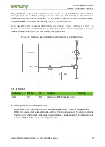
5.7.4 Antenna Assembly
The antenna used by the module must comply with the mobile device standards. The standing wave
ratio must be between 1.1 and 1.5, and the input impedance must be 50 Ω. Requirements for antenna
gain vary with the application environments. You can choose the appropriate antenna according to the
specific application scenario and environment.
Antenna interfaces can be connected to a rubber ducky antenna, magnet antenna, or embedded planar
inverted F antenna (PIFA). There must be good shielding between the external antenna and the RF
pin connection. Keep external RF cables far away from all interference sources, especially digital
signals and switch-mode power supply if using RF cables.
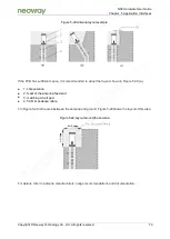
The following methods are commonly used to assemble antennas:
Module antenna using the RF cable connection method

