background image

19

CHAPTER  2    NAME AND FUNCTION OF COMPONENTS

This chapter describes the names, functions, and switch settings of components comprising the IE-703017-MC-

EM1.  For the details of the pod, jumpers, and switch positions, etc., refer to IE-703002-MC User’s Manual.

2.1

Component Name and Function of IE-703017-MC-EM1

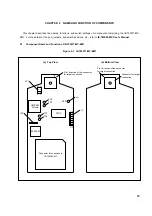
Figure 2-1.  IE-703017-MC-EM1

(a)  Top View

(b) Bottom View

Connector for cnnection to

IE-703002-MC

LED

V

PP

V850/SA1

I/O chip

Pin 1 direction of the connector 
for target connection

J1

FPGA

TP6

TP5

JP1

4

3

2

1

TP7

TP4

EEPROM

TM

Pin 1 direction of the connector 
for target connection

Connector for target 
connection

JP2

1

2

11

12

Содержание IE-703017-MC-EM1

Страница 1: ...Preliminary User s Manual Target device V850 SA1 IE 703017 MC EM1 In circuit Emulator Option Board 1 Document No U12898EJ1V0UM00 1st edition Date Published February 1998 N CP K Printed in Japan 1998 ...

Страница 2: ...2 MEMO ...

Страница 3: ... change without notice No part of this document may be copied or reproduced in any form or by any means without the prior written consent of NEC Corporation NEC Corporation assumes no responsibility for any errors which may appear in this document NEC Corporation does not assume any liability for infringement of patents copyrights or other intellectual property rights of third parties by or arisin...

Страница 4: ...onics Germany GmbH Duesseldorf Germany Tel 0211 65 03 02 Fax 0211 65 03 490 NEC Electronics UK Ltd Milton Keynes UK Tel 01908 691 133 Fax 01908 670 290 NEC Electronics Italiana s r 1 Milano Italy Tel 02 66 75 41 Fax 02 66 75 42 99 NEC Electronics Germany GmbH Benelux Office Eindhoven The Netherlands Tel 040 2445845 Fax 040 2444580 NEC Electronics France S A Velizy Villacoublay France Tel 01 30 67 ...

Страница 5: ...d switch settings of the IE 703002 MC when it is connected to the IE 703017 MC EM1 For the names and functions and the connection of components refer to the IE 703002 MC User s Manual Hardware To broadly learn about the basic specifications and operation methods Read this manual in the order listed in CONTENTS To learn the operation methods and command functions etc of the IE 703002 MC and IE 7030...

Страница 6: ...17 Data Sheet To be prepared µPD703017Y Data Sheet To be prepared Documents related to development tools User s Manual Product Document Number IE 703002 MC In circuit emulator U11595E IE 703017 MC EM1 In circuit emulator option board This manual Operation UNIX TM based U12839E Operation Windows TM based U12827E C language U12840E Assembly Language U10543E CA850 C Compiler package Project manager W...

Страница 7: ...ION OF COMPONENTS 19 2 1 Component Name and Function of IE 703017 MC EM1 19 2 2 Clock Settings 21 2 2 1 Main clock settings 21 2 2 2 Subclock settings 22 2 3 Illegal Access Detection ROM Setting 23 2 4 CPU Operation Voltage Range Switching Setting 23 2 5 Separate Bus Function Setting 24 CHAPTER 3 FACTORY SETTINGS 25 CHAPTER 4 CAUTIONS 27 4 1 VDD and BVDD of Target System 27 4 2 NMI Signal 28 4 3 V...

Страница 8: ...onfiguration 13 1 2 Contents in Carton 14 1 3 Accessories 15 1 4 Connection between IE 703002 MC and IE 703017 MC EM1 17 2 1 IE 703017 MC EM1 19 4 1 Schematic Diagram of Power Supply Acquisition 27 4 2 NMI Signal Flow Path 28 4 3 VPP Signal Flow Path 28 ...

Страница 9: ...Title Page 2 1 Main Clock Setting 21 2 2 Subclock Setting 22 2 3 JP1 setting in IE 703002 MC 23 2 4 JP3 and JP4 Setting in IE 703002 MC 23 2 5 MAM Register and J1 Setting Correspondence 24 4 1 Bus Interface Pin Operation List 29 ...

Страница 10: ...10 MEMO ...

Страница 11: ...02 MC Optional hardware CHAPTER 1 OVERVIEW The IE 703017 MC EM1 is an optional board for the IE 703002 MC in circuit emulator By connecting the IE 703017 MC EM1 and IE 703002 MC hardware and software can be debugged efficiently in system development using the V850 SA1 In this manual the basic setup sequences and switch settings of the IE 703002 MC when using IE 703017 MC EM1 are described For the ...

Страница 12: ...t 17 MHz operation frequency Note Height 15 mm Length 194 mm External dimensions Refer to APPENDIX DIMENSIONS Width 96 mm Weight 160 g Note 10 35 W when IE 703002 MC with IE 703017 MC EM1 1 3 Function Specifications When connected to IE 703002 MC Parameter Capacity Internal ROM 256 Kbytes In ROM less mode 2 Mbytes Emulation memory capacity External memory When using iROM 1 Mbyte Internal ROM 256 K...

Страница 13: ...2 MC optional 6 In circuit emulator option board IE 703017 MC EM1 7 External logic probe included with IE 703002 MC 8 Socket for target connection YQSOCKET100SDN included with IE 703002 MC 9 Extension probe SC 100SD optional 10 Connector for emulator connection YQPACK100SD included in IE 703002 MC 11 Connector for target connection NQPACK100SD included 12 Power adapter IE 70000 MC PS B optional 13...

Страница 14: ... that the accessory bag contains this manual and the connector accessories In case of missing or damaged contents please contact an NEC sales representative or NEC dealer Figure 1 2 Contents in Carton 1 IE 703017 MC EM1 1 pc 2 Accessory bag 1 pc 3 Guarantee card 1 pc 4 Packing list 1 sheet 1 IE 703017 MC EM1 2 Accessory bag 3 Guarantee card 4 Packing list ...

Страница 15: ... 1 set including NQGUIDE 3 pcs screw driver 1 pc b Crystal oscillator 17 MHz 8 pin type 1 pc c Plastic screws 4 pcs including nuts and washer 4 sets Figure 1 3 Accessories Caution NQPACK100SD is intended for program development and evaluation in laboratories a Connector for target connection NQPACK100SD Side View NQGUIDE Driver b Crystal oscillator c Plastic screw ...

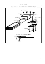
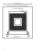
Страница 16: ...od refer to Figure 1 4 c When connecting position the IE 703002 MC and IE 703017 MC EM1 so that they are horizontal 5 Set the PGA socket lever of the IE 703017 MC EM1 to the CLOSE position as shown in Figure 1 4 b 6 Set the jumpers JP1 to JP4 Open JP1 and JP3 Remove the jumper contact Attach the removed jumper contact to one of the jumper pins to avoid losing them Retain the factory settings of JP...

Страница 17: ...7 Figure 1 4 Connection between IE 703002 MC and IE 703017 MC EM1 1 2 a Overview b PGA Socket Lever of IE 703017 MC EM1 CLOSE OPEN IE 703002 MC Nylon rivets Upper cover Nut Washer IE 703017 MC EM1 Lower cover Plastic screw ...

Страница 18: ...CHAPTER 1 OVERVIEW 18 Figure 1 4 Connection between IE 703002 MC and IE 703017 MC EM1 2 2 c Connecting part IE 703017 MC EM1 Pin A1 location Insertion guide IE 703002 MC insertion area ...

Страница 19: ...etc refer to IE 703002 MC User s Manual 2 1 Component Name and Function of IE 703017 MC EM1 Figure 2 1 IE 703017 MC EM1 a Top View b Bottom View Connector for cnnection to IE 703002 MC LED VPP V850 SA1 I O chip Pin 1 direction of the connector for target connection J1 FPGA TP6 TP5 JP1 4 3 2 1 TP7 TP4 EEPROMTM Pin 1 direction of the connector for target connection Connector for target connection JP...

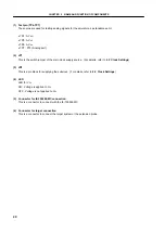
Страница 20: ...main clock supply source For details refer to 2 2 Clock Settings 3 JP2 This is a pin block for supplying the subclock For details refer to 2 2 Clock Settings 4 LED LED for VPP ON Voltage is applied to VPP OFF Voltage is not applied to VPP 5 Connector for IE 703002 MC connection This is a connector to connect with the IE 703002 MC 6 Connector for target connection This is a connector to connect the...

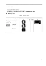
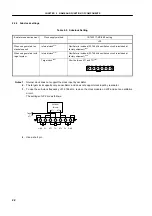
Страница 21: ...position in the IE 703002 MC refer to IE 703002 MC User s Manual 2 2 1 Main clock settings Table 2 1 Main Clock Setting IE 703017 MC EM1 setting IE 703002 MC setting Emulator use environment Clock supply method JP1 SW1 SW2 JP2 When using emulator as standalone unit Internal clock 4 3 2 1 Internal clock 4 3 2 1 When using emulator with target system Target clock 4 3 2 1 ON ON 8 7 2 1 ...

Страница 22: ...2 768 kHz oscillation circuit is included at factory shipment Note 3 When using emulator with target system Target clockNote 2 Short between XT1 and TGNote 4 GND C1 XT1 TG XT2 C2 GND Notes 1 Internal clock does not support the clock input by oscillator 2 The target clock supports only an oscillator and does not support clock input by resonator 3 To use the sub clock frequency of 32 768 kHz remove ...

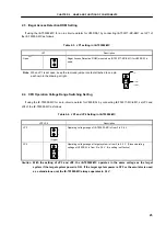
Страница 23: ...e Range Switching Setting If using the IE 703002 MC for an in circuit emulator for V850 SA1 by connecting IE 703017 MC EM1 set JP3 and JP4 of the IE 703002 MC as follows Table 2 4 JP3 and JP4 Setting in IE 703002 MC JP3 JP4 Description JP3 1 2 Open Operating voltage range of IE 703002 MC is from 2 to 3 6 V JP4 1 2 3 Operating voltage range of target system is from 2 to 4 5 V Since operating voltag...

Страница 24: ...113 J1 Setting P34 P36 Port mode P100 P107 Port mode 0 0 0 P110 P113 Port mode 2 1 12 11 P34 P36 Port mode P100 P107 Port mode 0 1 0 P110 P113 A1 A4 2 1 12 11 P34 P36 Port mode P100 P103 A5 A8 P104 P107 Port mode 0 1 1 P110 P113 A1 A4 2 1 12 11 P34 P36 Port mode P100 P107 A5 A12 1 0 0 P110 P113 A1 A4 2 1 12 11 P34 A13 P35 P36 Port mode P100 P107 A5 A12 1 0 1 P110 P113 A1 A4 2 1 12 11 P34 P35 A13 A...

Страница 25: ...3 FACTORY SETTINGS Pin Description Remark JP1 4 3 2 1 Internal main clock setting JP2 Oscillation circuit is set 32 768 kHz clock is supplied for subclock J1 1 2 11 12 Set to port mode P34 P36 P100 P107 P110 P113 ...

Страница 26: ...26 MEMO ...

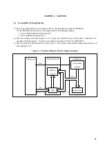
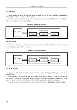
Страница 27: ...age of the target system is 1 V or higher the evaluation chip in the emulator is supplied VDD to operate by the target system The power consumption is equivalent to that of the µPD70F3017 3 When the voltage of the target system is lower than 1 V the emulator recognizes the target system power is off and operates at 3 3 V Figure 4 1 Schematic Diagram of Power Supply Acquisition BVDD 1 V IE 703002 M...

Страница 28: ...the emulator It is not connected to the evaluation chip in the emulator Figure 4 3 VPP Signal Flow Path Evaluation chip IE 703017 MC EM1 VPP signal Target system 330 Ω LED 4 4 MAM Register Debugging of MAM register cannot be performed in the emulator If debugging MAM register with software proceed with care In the target device the port can be used as an address bus by setting a value to the MAM r...

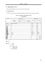
Страница 29: ... Memory used by emulator Internal ROM Internal RAM Internal Peripheral I O Emulation RAM Target System Pin name F R W R R W R W R W R W A16 A21 Hold the accessed last Active Active AD0 AD15 Hi Z Active Active ASTB H Active Active R W H Active Active DSTB H H Active LBEN H Active Active UBEN H Active Active WAIT Invalid Maskable Maskable HLDRQ Maskable Maskable Maskable HLDAK H or L H or L H or L W...

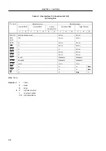
Страница 30: ...W F R W A16 A21 Hold the accessed last Active Active AD0 AD15 Hi Z Active Active ASTB H Active Active R W H Active Active DSTB H H Active LBEN H Active Active UBEN H Active Active WAIT Invalid Maskable Maskable HLDRQ Maskable Maskable Maskable HLDAK H or L H or L H or L WRL H H H Note WRH H H H Note RD H H Note H Note Active Remarks 1 F Fetch R Read W Write 2 H High level output L Low level output...

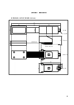
Страница 31: ...1 APPENDIX DIMENSIONS IE 703002 MC IE 703017 MC EM1 Unit mm 481 103 166 58 8 52 90 27 212 Top View Side View IE 703017 MC EM1 IE 703002 MC Bottom View Top View 14 5 194 29 0 96 37 5 29 0 Pin 1 direction ...

Страница 32: ...32 MEMO ...

Страница 33: ...erica NEC Electronics Inc Corporate Communications Dept Fax 1 800 729 9288 1 408 588 6130 Europe NEC Electronics Europe GmbH Technical Documentation Dept Fax 49 211 6503 274 South America NEC do Brasil S A Fax 55 11 6465 6829 Asian Nations except Philippines NEC Electronics Singapore Pte Ltd Fax 65 250 3583 Japan NEC Corporation Semiconductor Solution Engineering Division Technical Information Sup...

Отзывы: