L M X 2 5 3 1 L Q 1 1 4 6 E E V A L U A T I O N B O A R D O P E R A T I N G I N S T R U C T I O N S
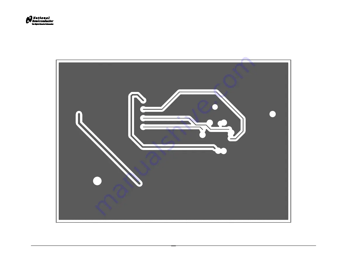
Mid Layer 2 "Power"
21
Страница 1: ...2531LQ1146E Evaluation Board Operating Instructions National Semiconductor Corporation Timing Devices Business Group 10333 North Meridian Suite 400 Indianapolis IN 46290 LMX2531LQ1146EFPEB Rev 3 31 20...
Страница 2: ...IVIDE BY 2 DISABLED 6 FREE RUNNING VCO PHASE NOISE INTERNAL DIVIDE BY 2 ENABLED 7 FRACTIONAL SPURS INTERNAL DIVIDE BY 2 DISABLED 8 FRACTIONAL SPURS INTERNAL DIVIDE BY 2 ENABLED 9 INTEGER SPURS INTERNA...
Страница 3: ...tend to be very noisy and should be used with caution If a signal generator is used the signal generator phase noise contribution can be reduced by setting the signal to 80 MHz and dividing this down...
Страница 4: ...l generator is used ensure that the RF is set to ON If using the lower frequency band DIV2 1 the VCO frequency in CodeLoader should be twice the frequency at the Fout pin Ensure that the VCO FREQUENCY...
Страница 5: ...1 4 6 E E V A L U A T I O N B O A R D O P E R A T I N G I N S T R U C T I O N S Phase Noise Output Frequency 1146 MHz Internal Divide by 2 Disabled DIV2 0 Output Frequency 573 MHz Internal Divide by...
Страница 6: ...f the VCO In order to take these plots the E5052 phase nose analyzer was used The method was to lock the PLL to the proper frequency then disable the EN_PLL EN_PLLLDO1 and EN_PLLLDO2 bits The equipmen...
Страница 7: ...was to lock the PLL to the proper frequency then disable the EN_PLL EN_PLLLDO1 and EN_PLLLDO2 bits The equipment needs to be able to track the VCO phase noise to measure in this way and one can not le...
Страница 8: ...se frequency of 1110 25 MHz is 78 6 dBc Worst case channels occur at exactly one channel spacing above or below a multiple of the crystal frequency Fractional Spur at 250 kHz offset at a worst case fr...
Страница 9: ...Hz offset at a frequency of 555 125 MHz is 92 5 dBc Since this mode uses the divide by 2 mode the channel spacing here is actually 125 kHz The spur at 125 kHz could be completely eliminated changing t...
Страница 10: ...T R U C T I O N S Integer Spurs Internal Divide by 2 Disabled Spur at 10 MHz offset for a frequency of 1106 MHz is 94 7 dBc Spur at 10 MHz offset for a frequency of 1146 MHz is 93 2 dBc Spur at 10 MHz...
Страница 11: ...rs Internal Divide by 2 Enabled Spur at 10 MHz offset for a frequency of 553 MHz is below the spectrum analyzer noise floor Spur at 10 MHz offset for a frequency of 573 MHz is below the spectrum analy...
Страница 12: ...Q 1 1 4 6 E E V A L U A T I O N B O A R D O P E R A T I N G I N S T R U C T I O N S CodeLoader Settings CodeLoader runs many devices When CodeLoader is first started it is necessary to select the cor...
Страница 13: ...gs and frequencies but not the Port Setup information For the CodeLoader program the default reference oscillator used for these instructions was 10 MHz but there is a mode for a 61 44 MHz oscillator...
Страница 14: ...bit to view more information about what this does When the DIV2 bit is enabled the frequency from the part will be half of that shown on the PLL VCO tab The frequency on the PLL VCO tab does not refl...
Страница 15: ...N S The Registers tab shows the literal bits that are being sent to the part These are the registers every time the PLL is loaded by using the menu command or Ctrl L R5 INIT1 and R5 INIT 2 are just th...
Страница 16: ...R A T I N G I N S T R U C T I O N S The port setup tells CodeLoader what information goes where If this is wrong the part will not program Although LPT1 is usually correct CodeLoader does NOT automati...
Страница 17: ...C1 R2 C12 C2 VccVCO VccDIG VccPLL VccBUF R3 C3 C17 R4 C9 C4 R5 C5 OSCin VccVCO VccPLL VccBUF C13 C18 C20 R7 R23 R22 Ftest LD C15 C22 R1 R9 TRIGGE R GND 1 2 3 4 5 6 7 8 POWER C24 C14 C11 C19 C21 C23 No...
Страница 18: ...9 2 Panasonic P 22AHCT ND 603 10 0 1W Thick Film 0 22 R22 R23 10 2 Vishay CRCW06033R3JRT1 603 5 0 1W Thick Film 3 3 R1 R18 11 4 Vishay CRCW0603100JRT1 603 5 0 1W Thick Film 10 R2 R3 R4 R5 12 1 Vishay...
Страница 19: ...L M X 2 5 3 1 L Q 1 1 4 6 E E V A L U A T I O N B O A R D O P E R A T I N G I N S T R U C T I O N S Top Layer 19...
Страница 20: ...L M X 2 5 3 1 L Q 1 1 4 6 E E V A L U A T I O N B O A R D O P E R A T I N G I N S T R U C T I O N S Mid Layer 1 Ground Plane 15 Mils Down FR4 20...
Страница 21: ...L M X 2 5 3 1 L Q 1 1 4 6 E E V A L U A T I O N B O A R D O P E R A T I N G I N S T R U C T I O N S Mid Layer 2 Power 21...
Страница 22: ...L M X 2 5 3 1 L Q 1 1 4 6 E E V A L U A T I O N B O A R D O P E R A T I N G I N S T R U C T I O N S Bottom Layer Signal Note Total Board Thickness 61 mils 22...
Страница 23: ...L M X 2 5 3 1 L Q 1 1 4 6 E E V A L U A T I O N B O A R D O P E R A T I N G I N S T R U C T I O N S Top Build Diagram 23...
Страница 24: ...or use in safety critical applications such as life support where a failure of the TI product would reasonably be expected to cause severe personal injury or death unless officers of the parties have...