


http://www.national.com
10
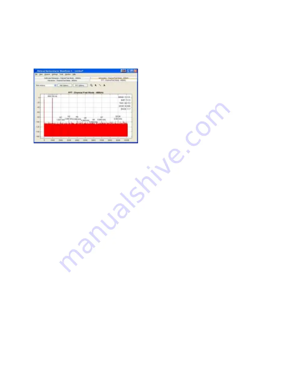
To view an FFT of the data captured, click on the
‘FFT’ tab. This plot may be zoomed in on the data
plot. A display of dynamic performance
parameters in the form of SINAD, SNR, THD,
SFDR and ENOB will be displayed at the top right
hand corner of the FFT plot (
Figure 13
).
Figure 13: FFT: 1kHz Sine Wave Input
Acquired data may be saved to a file. Plots may
also be exported as graphics. See the Data
Capture Board User's Guide for details.
5.3 Register Control
The ADC’s internal registers are controlled
through the ADC121C021 Control Panel
(
see Figure 7
). WaveVision allows both read and
write access to these registers. To read the
registers, simply click the “Read All” button in the
Control Panel window. Each of the registers is
read and displayed in the control panel. To write
to a register, simply type in the 8-bit or 16-bit hex
value to be written to the register and press Enter.
All hex values are assumed to be right justified.
Zeros are written to unspecified bits.
Many functions of the ADC121C021 are enabled
through the internal registers. Please refer to
Section 1.6
on Internal Registers in the Datasheet
for further details.
For example, the following steps will enable the
ALERT pin, set the V
LOW
threshold to ¾ full-scale,
and create an Under Range Alert condition.
-Write 0x04 to the Configuration register.
-Write 0xBFF to the V
LOW
register.
-Ground the analog input (V
IN
).
-Click the “Read Registers” button to read all the
registers.
-The Alert Status register will read 01hex to
indicate that the V
LOW
value was violated and an
Under Range Alert condition has occurred.