3.
Repeat steps 1 and 2 to synchronize additional USRP RIO devices using the additional
ports on the CDA-2990 (optional).
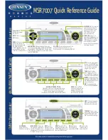
The completed hardware setup for two USRP RIO devices is shown in the following
figure.
Figure 3. Synchronizing Multiple USRP RIO Devices with the CDA-2990
CDA-2990
Designed by Ettus Research
Designed by Ettus Research
3
4
5
6
2
1
7
8
7
8
3
4
5
6
2
1
PPS OUT
10 MHz OUT
PPS OUT
POWER
GPS LOCK
PPS
STATUS
EXTERNAL
INTERNAL
ETHERNET
GPS ANT
INPUT
PRIMARY REF
INTERNAL
EXTERNAL
EXT 10 MHz
INPUT
EXT PPS
INPUT
POWER
8 Channel Clock Distribution Module
6
–
15 V
6 W MAX
0
1
PWR
REF
IN
PPS
OUT
TRIG
5V DC
REF
OUT
1G/10G ETH
3.3 V
+15 dBm
MAX
9-16V DC
7.5 A MAX
SFP+Ports
PCIe x4
TRIG
3.3V
IN
5V MAX
PPS
GPS
ANT
–15 dBm
MAX
0
1
PWR
REF
IN
PPS
OUT
TRIG
5V DC
REF
OUT
1G/10G ETH
3.3 V
+15 dBm
MAX
9-16V DC
7.5 A MAX
SFP+Ports
PCIe x4
TRIG
3.3V
IN
5V MAX
PPS
GPS
ANT
–15 dBm
MAX
Standard
SMA-SMA
Cables
10 MHz
PPS
Preparing the USRP-2945 for LO Sharing (Optional)
Complete the following steps to prepare a single USRP-2945 device to share local oscillators
(LOs) among all four channels in the device.
1.
Connect the LO OUT 1 IF2 connector of the USRP-2945 back panel to the LO IN 0 IF2
connector of the same USRP-2945 back panel using an SMA(m)-to-SMA(m) cable.
2.
Connect the LO OUT 1 IF1 connector of the USRP-2945 back panel to the LO IN 0 IF1
connector of the same USRP-2945 back panel using an SMA(m)-to-SMA(m) cable.
The completed hardware setup is shown in the following figure.
Figure 4. USRP-2945 Single Device LO Sharing
0
1
PWR
1G/10G ETH
9-16V DC
7.5 A MAX
SFP+Ports
1
1. SMA(m)-to-SMA(m) Cables
USRP-2940/2942/2943/2944/2945 Getting Started Guide
|
© National Instruments
|
7