background image

PXIe-5185/5186 Calibration Procedure 

|

  © National Instruments 

|

  9

7.

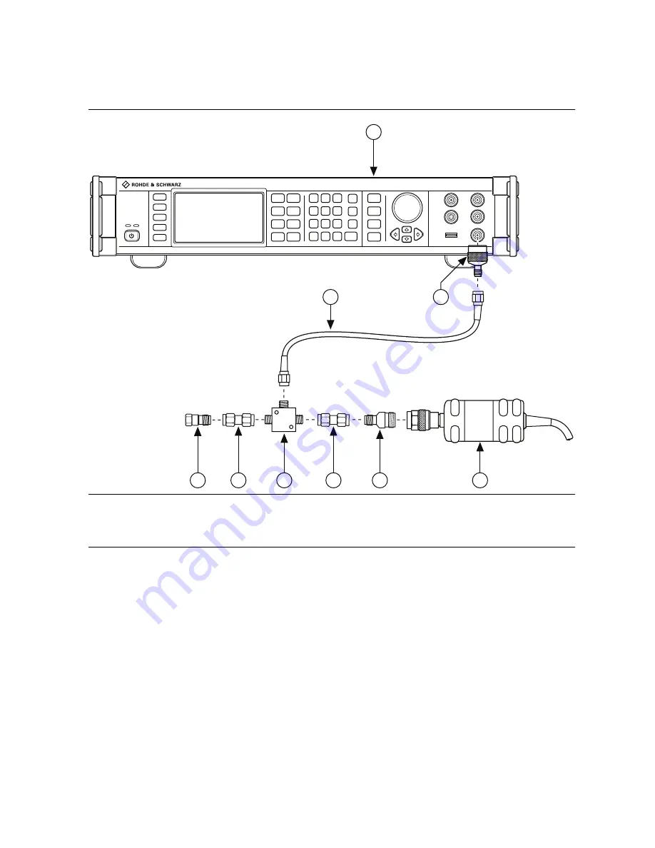
Connect the power sensor to splitter output 2.

The following figure illustrates the hardware setup.

Figure 1.  

Connection Diagram for Measuring at Splitter Output 2 (SMA)

8.

Configure the signal generator to generate a sine waveform with the following 
characteristics:

Frequency: the Test Point Frequency value from Table 2

Amplitude level: the Test Point Amplitude value from Table 2

9.

Configure the power sensor to correct for the Test Point Frequency value using the power 
sensor frequency correction function.

10. Use the power sensor to measure the power in dBm.
11. Repeat steps 8 through 10 for each configuration in Table 2, recording each result as 

splitter output 2 power

, where each configuration has a corresponding value.

12. Disconnect the power sensor and 50 

Ω

 SMA terminator (f) from splitter output 2 and 

splitter output 1.

1

Signal Generator

2

SMA (f)-to-N (m) Adapter

3

SMA (m)-to-SMA (m) Cable

4

50 

Ω

SMA Terminator (f)

5

SMA (m)-to-SMA (m) Adapter

6

Power Splitter

7

SMA (f)-to-N (f) Adapter

8

Power Sensor

1

6

4

5

3

7

8

2

5

Содержание PXIe-5185

Страница 1: ...visit ni com calibration Contents 50 Ω and 1 MΩ Devices 2 Software Requirements 2 Related Documentation 2 Password 3 Calibration Interval 3 Test Equipment 3 Test Conditions 5 Calibration Procedures 6 Initial Setup 6 Self Calibration 6 MAX 7 NI SCOPE Soft Front Panel 7 NI SCOPE 7 External Calibration 7 Test System Characterization 7 Zeroing the Power Sensor 8 Characterizing Power Splitter Amplitude...

Страница 2: ...SCOPE supports programming a self calibration and an external calibration in multiple application development environments ADEs When you install NI SCOPE you need to install support for only the ADE that you intend to use LabVIEW support is in the niScope llb file and all calibration functions appear in the NI SCOPE Calibration palette For LabWindows CVI users the NI SCOPE function panel niScope f...

Страница 3: ...dard Table 1 PXIe 5185 5186 Test Equipment Equipment Recommended Model Requirements Oscilloscope calibrator Fluke 9500B 3200 DC Output Range 2 V to 2 V into 50 Ω 6 5V to 6 5 V into 1 MΩ DC Voltage Accuracy DC 0 3 of output into 50 Ω and 1 MΩ Leveled Sine Wave Amplitude Range 0 9 Vpk pk into 50 Ω Leveled Sine Wave Frequency Accuracy 4 ppm Square Wave 8 0 Vpk pk at 100 kHz into 1 MΩ 3 2 GHz output m...

Страница 4: ...1852F Frequency range DC to 5 0 GHz VSWR 1 1 Impedance 50 Ω SMA m to SMA m cable Frequency range DC to 5 0 GHz VSWR 1 1 Length 1 meter SMA m to BNC f Fairview Microwave SM4723 Frequency range DC to 100 kHz Impedance 50 Ω SMA f to N m adapter Fairview Microwave SM4226 Frequency range DC to 5 0 GHz VSWR 1 05 Impedance 50 Ω SMA f to N f adapter Fairview Microwave SM4236 Frequency range DC to 5 0 GHz ...

Страница 5: ...ng temperature Ensure that the PXI Express chassis fan speed is set to HIGH that the fan filters are clean if present and that the empty slots contain PXI chassis slot blockers and filler panels For more information refer to the Maintain Forced Air Cooling Note to Users document available at ni com manuals Plug the chassis PC and the calibrator into the same power strip to avoid ground loops BNC f...

Страница 6: ...ing sections Initial Setup Refer to the NI High Speed Digitizers Getting Started Guide for information about how to install the software and hardware and how to configure the device in MAX Self Calibration The PXIe 5185 5186 includes precise internal circuits and references used during self calibration to adjust for any errors caused by short term fluctuations in the environment Note Allow a 25 mi...

Страница 7: ...t is the process of measuring and compensating for device performance to improve the input accuracy Performing an adjustment updates the calibration date resetting the calibration interval The device is warranted to meet or exceed its published specifications for the duration of the calibration interval Test System Characterization The following procedures characterize the test equipment used duri...

Страница 8: ...ct the RF OUT connector of the signal generator to the input port of the power splitter using an SMA f to N m adapter and an SMA m to SMA m cable 4 Connect an SMA m to SMA m adapter to one of the power splitter output ports Refer to this assembly as splitter output 1 5 Connect the 50 Ω SMA terminator f to splitter output 1 6 Connect the other SMA m to SMA m adapter to the other output port of the ...

Страница 9: ...e 2 9 Configure the power sensor to correct for the Test Point Frequency value using the power sensor frequency correction function 10 Use the power sensor to measure the power in dBm 11 Repeat steps 8 through 10 for each configuration in Table 2 recording each result as splitter output 2 power where each configuration has a corresponding value 12 Disconnect the power sensor and 50 Ω SMA terminato...

Страница 10: ...e waveform with the following characteristics Frequency the Test Point Frequency value from Table 2 Amplitude level the Test Point Amplitude value from Table 2 16 Configure the power sensor to correct for the Test Point Frequency value using the power sensor frequency correction function 17 Use the power sensor to measure the power in dBm 1 Signal Generator 2 SMA f to N m Adapter 3 SMA m to SMA m ...

Страница 11: ...of this characterization are later used as a correction in the Verifying 1 MΩ AC Amplitude Accuracy and Bandwidth procedure 1 Connect the BNC f to N f adapter to the power sensor Refer to this assembly as the power sensor 2 Zero the power sensor as described in the Zeroing the Power Sensor section 3 Connect the RF OUT connector of the signal generator to the input port of the power splitter using ...

Страница 12: ...Configure the power sensor to correct for the Test Point Frequency value using the power sensor frequency correction function 10 Use the power sensor to measure the power in dBm 11 Repeat steps 8 through 10 for each configuration in Table 3 recording each result as splitter output 2 power where each configuration has a corresponding value 12 Disconnect the power sensor and 50 Ω BNC terminator f fr...

Страница 13: ...uency value from Table 3 Amplitude level the Test Point Amplitude value from Table 3 16 Configure the power sensor to correct for the Test Point Frequency value using the power sensor frequency correction function 17 Use the power sensor to measure the power in dBm 18 Repeat steps 15 through 17 for each configuration in Table 3 recording each result as splitter output 1 power where each configurat...

Страница 14: ...accuracy of the PXIe 5185 5186 compare the voltage measured by the device and the value sourced by the voltage standard Table 5 lists the settings for each channel 1 Connect the calibrator test head directly to the channel 0 50 Ω input of the PXIe 5185 5186 2 Configure the PXIe 5185 5186 with the following settings Vertical coupling DC Table 4 Verification Tests Test Type Specification Recommended...

Страница 15: ... steps 2 8 for iterations 2 through 16 listed in Table 5 10 Connect the calibrator test head directly to the channel 1 50 Ω input of the PXIe 5185 5186 and repeat steps 2 through 9 Note If your module supports 1 MΩ input follow steps 11 and 12 Otherwise DC and programmable vertical offset accuracy has been verified 1 MΩ input is available on PXIe 5185 module part number 152962x 0zL and PXIe 5186 m...

Страница 16: ... 17 1 MΩ 0 11 0 0 045 0 0032 18 1 MΩ 0 11 0 0 045 0 0032 19 1 MΩ 0 11 0 25 0 295 0 0112 20 1 MΩ 0 11 0 25 0 295 0 0112 21 1 MΩ 0 2 0 0 08 0 0047 22 1 MΩ 0 2 0 0 08 0 0047 23 1 MΩ 0 2 0 25 0 33 0 0127 24 1 MΩ 0 2 0 25 0 33 0 0127 25 1 MΩ 0 5 0 0 2 0 0098 26 1 MΩ 0 5 0 0 2 0 0098 27 1 MΩ 0 5 0 25 0 45 0 0178 28 1 MΩ 0 5 0 25 0 45 0 0178 29 1 MΩ 1 0 0 4 0 0183 30 1 MΩ 1 0 0 4 0 0183 Table 5 PXIe 5185...

Страница 17: ... of the power sensor assembly from the Test System Characterization section to the channel 0 50 Ω input of the PXIe 5185 5186 31 1 MΩ 1 0 25 0 65 0 0263 32 1 MΩ 1 0 25 0 65 0 0263 33 1 MΩ 2 0 0 8 0 0353 34 1 MΩ 2 0 0 8 0 0353 35 1 MΩ 2 2 5 3 3 0 1153 36 1 MΩ 2 2 5 3 3 0 1153 37 1 MΩ 5 0 2 0 0863 38 1 MΩ 5 0 2 0 0863 39 1 MΩ 5 2 5 4 5 0 1663 40 1 MΩ 5 2 5 4 5 0 1663 41 1 MΩ 10 0 4 0 1713 42 1 MΩ 10...

Страница 18: ...rdware setup Figure 5 50 Ω AC Amplitude Accuracy and Bandwidth Verification Cabling Diagram 1 Power Sensor 2 SMA f to N f Adapter 3 SMA m to SMA m Adapter 4 Power Splitter 5 PXIe 5185 5186 6 SMA m to SMA m Cable 7 SMA f to N m Adapter 8 Signal Generator 3 GHz 12 5 GS s 8 Bit Digitizer ACCESS ACTIVE REF CLK CLK IN 16 dBm Max 1 4 Vrms 50 9 dBm Max 0 6 Vrms 50 1 Vpp measure 1 V MAX 1 Vpp measure 1 V ...

Страница 19: ...ints from the Test System Characterization section for the current Test Point frequency from Table 6 7 Use the PXIe 5185 5186 to acquire and measure the power using the Extract Single Tone Information VI converting the result from Vpk to dBm Record the result as device input power 8 If the Test Point frequency from Table 6 is 50 kHz proceed to the following step Otherwise go to step 12 9 Calculate...

Страница 20: ...er splitter 1 Connect the 50 Ω BNC feed through terminator to the channel 0 1 MΩ input of the PXIe 5185 5186 Connect splitter output 2 of the power sensor assembly from the Test System Characterization section to the 50 Ω BNC feed through terminator Note The power sensor assembly must match the configuration used in the Test System Characterization section in which the power sensor is connected to...

Страница 21: ...pedance 1 MΩ 1 Power Sensor 2 BNC m to N m Adapter 3 SMA f to BNC f Adapter 4 Power Splitter 5 50 Ω BNC Feed Through 6 PXIe 5185 5186 7 SMA f to SMA f Cable 8 SMA m to N f Adapter 9 Signal Generator 3 GHz 12 5 GS s 8 Bit Digitizer ACCESS ACTIVE REF CLK CLK IN 16 dBm Max 1 4 Vrms 50 9 dBm Max 0 6 Vrms 50 1 Vpp measure 1 V MAX 1 Vpp measure 1 V MAX 10 Vpp measure 42 V MAX 10 Vpp measure 42 V MAX CH ...

Страница 22: ...e PXIe 5185 5186 to acquire and measure the power using the Extract Single Tone Information VI converting the result from Vpk to dBm Record the result as device input power 8 If the Test Point frequency from Table 7 is 50 kHz proceed to step 9 Otherwise go to step 12 9 Calculate the power reference using the following equation power reference device input power corrected input power 10 Compare the...

Страница 23: ... s for settling then record the measured peak frequency 7 Use the following formula to calculate the frequency difference TBerror f 1 0E 9 1 0E 3 where f measured frequency 8 Compare the error to the Test Limit shown in Table 8 Note Timebase verification is only required on one channel Adjustment If the PXIe 5185 5186 successfully passed each of the verification procedures within the test limits t...

Страница 24: ... through 8 changing the value of the channels parameter from 0 to 1 Note If your module supports 1 MΩ input follow steps 10 through 22 Otherwise jump to step 23 to complete the adjustment 1 MΩ input available on PXIe 5185 module part number 152962X 0ZL and PXIe 5186 module part number 152961X 0ZL where X is any letter and Z is any number 10 Connect the calibrator test head directly to the channel ...

Страница 25: ...irectly to the channel 1 1 MΩ input of the digitizer and repeat steps 11 through 21 changing the value of the channels parameter from 0 to 1 23 Connect the calibrator test head directly to the external trigger channel input on the digitizer 24 Configure the calibrator output impedance to 50 Ω 25 Configure the calibrator to output the voltage listed under Input V in Table 11 for the current iterati...

Страница 26: ...ion section to reverify the performance of the digitizer after adjustments LabVIEW VI C C Function Call CallniScope_CalAdjustRangewith the following parameters vi The instrument handle from niScope_CalStart channelName NISCOPE_VAL_EXTERNAL range 0 stimulus The Input V value listed in Table 11 for the current iteration LabVIEW VI C C Function Call Call niScope_CalSelfCalibrate with the following pa...

Страница 27: ...Channel External Adjustment Iteration Input V 1 0 32 2 0 135 3 0 075 4 0 065 5 0 055 6 0 045 7 0 045 8 0 055 9 0 065 10 0 075 11 0 135 12 0 32 13 2 0 14 2 0 Table 10 PXIe 5185 5186 1 MΩ Input Parameters for Input Channel External Adjustment Iteration Input V 1 5 0 2 3 0 3 2 0 4 1 0 5 0 75 6 0 5 7 0 32 8 0 135 9 0 075 ...

Страница 28: ...0 075 17 0 135 18 0 32 19 0 5 20 0 75 21 1 0 22 2 0 23 3 0 24 5 0 Table 11 PXIe 5185 5186 Input Parameters for External Trigger Channel External Adjustment Iteration Input V 1 5 0 2 0 001 3 5 0 Table 10 PXIe 5185 5186 1 MΩ Input Parameters for Input Channel External Adjustment Continued Iteration Input V ...

Страница 29: ...Services The NI website is your complete resource for technical support At ni com support you have access to everything from troubleshooting and application development self help resources to email and phone assistance from NI Application Engineers Visit ni com services for NI Factory Installation Services repairs extended warranty and other services Visit ni com register to register your NI produ...

Отзывы: