


Appendix B
Timing Diagrams
B-34
ni.com
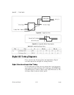
Counters Timing Diagrams
This section describes input delays, input requirements, output delays,
gating modes, and quadrature and two pulse encoder timing.
Input Delays
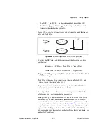
This section describes some of the timing delays of the counter/timer
circuit. To describe delays of the counter/timer, we model the circuitry as
shown in Figure B-41. In the figure, PFI, RTSI, and PXI_STAR represent
signals at connectors pins of the M Series device. The other named signals
represent internal signals.
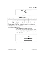
Table B-24.
DO Timing Delays
Time
From
To
Min (ns)
Max (ns)
t
12
*
PFI
PFI_i
5.2
6.2
18.2
22.0
RTSI
RTSI_i
2.0
2.5
5.0
6.0
PXI_STAR
PXI_STAR_i
1.5
3.5
t
13
PFI_i, RTSI_i, PXI_STAR_i, or
other internal signal
DO Sample Clock
3.5
9.5
t
14
DO Sample Clock
P0
7.5
27.5
t
15
DO Sample Clock
PFI (output)
8.0
29.8
t
16
†
PFI (output) high
PFI (output) low
Two periods of
80 MHz Timebase
Three periods of
80 MHz Timebase
*
The delay ranges given for PFI and RTSI represent the fastest and slowest terminal routing within the trigger group for a
given condition (maximum or minimum timing). This difference can be useful when two external signals will be used
together and the relative timing between the signals is important.
†
When DO Sample Clock is routed to a PFI output pin, the pulse width of the output is independent of the pulse width of
the input. The pulse width is specified in a number of periods of the 80 MHz Timebase.
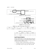
Table B-25.
DO Timing Requirements
Time
Requirement
Condition
Min (ms)
Max (ms)
t
10
PFI, RTSI, or PXI_STAR
Minimum Period
When used as
DO Sample Clock
NI 622
x
devices: 1000.0
NI 625
x
/NI 628
x
devices: 100.0
—
t
11
PFI, RTSI, or PXI_STAR
Minimum Pulse Width
When used as
DO Sample Clock
12.0
—


