background image

Chapter 4

Signal Connections

©

 National Instruments Corporation

4-7

PCI-4451/4452/4453/4454 User Manual

Table 4-4.  

Analog I/O Signal Summary for the PCI-4453/4454

Signal Name

Signal 

Type and 
Direction

Impedance 

Input/

Output

Protection 

(Volts) 

On/Off

Source 
(mA at 

V)

Sink 

(mA at 

V)

Rise 

Time 

(ns)

Bias

+ACH<0..3>

AI

1 M


in parallel with 
50 pF to 
AIGND

±42.4 V/±42.4 V

±100 pA

AO_SHLD <0..3>

CGND

+DAC0OUT

AO

22 

 to 

AOGND

Short-circuit to 
ground

16.7 mA 
at 10 V

+DAC1OUT 

AO

22 

Ω 

to 

AOGND

Short-circuit to 
ground

16.7 mA 
at 10 V

AO_SHLD <0..1>

DGND

DIO

+5 V

DO

0.7 

Short-circuit to 
ground

1 A

AI = Analog Input

AO = Analog Output

DIO = Digital Input/Output

DO = Digital Output

 ±400 V/±400 V guaranteed by design, but not tested or certified to operate beyond ±42.4 V

Содержание DAQ PCI-4451

Страница 1: ...DAQ PCI 4451 4452 4453 4454 User Manual Dynamic Signal Acquisition Device for PCI PCI 4451 4452 4453 4454 User Manual March 2000 Edition Part Number 321891B 01...

Страница 2: ...many 089 741 31 30 Greece 30 1 42 96 427 Hong Kong 2645 3186 India 91805275406 Israel 03 6120092 Italy 02 413091 Japan 03 5472 2970 Korea 02 596 7456 Mexico D F 5 280 7625 Mexico Monterrey 8 357 7695...

Страница 3: ...ure to follow the National Instruments installation operation or maintenance instructions owner s modification of the product owner s abuse misuse or negligent acts and power failure or surges fire fl...

Страница 4: ...DAQ Driver Software 1 4 Optional Equipment 1 5 Custom Cabling 1 6 Analog Cables 1 6 Analog Accessories 1 7 Digital Cables PCI 4451 4452 Only 1 7 Chapter 2 Installation and Configuration Software Insta...

Страница 5: ...gnal Connections PCI 4451 4452 Only 4 17 Digital Power Connections PCI 4451 4452 Only 4 18 Timing Connections 4 18 Programmable Function Input Connections PCI 4451 4452 Only 4 19 Acquisition Timing Co...

Страница 6: ...on 5 3 Chapter 6 Theory of Analog Operation Functional Overview 6 1 Analog Input Circuitry 6 1 Input Coupling 6 3 Calibration 6 3 Antialias Filtering 6 3 The ADC 6 9 Noise 6 10 Analog Output Circuitry...

Страница 7: ...54 4 13 Figure 4 6 Analog Output Channel Block Diagram for the PCI 4451 4 15 Figure 4 7 Analog Output Channel Block Diagram for the PCI 4453 4 16 Figure 4 8 Digital I O Connections 4 17 Figure 4 9 Typ...

Страница 8: ...e and Resolution of the PCI 4451 3 7 Table 4 1 Analog I O Connector Pin Assignment for the PCI 4451 4452 4 3 Table 4 2 Analog I O Signal Summary for the PCI 4451 4452 4 4 Table 4 3 Analog I O Connecto...

Страница 9: ...e the manuals you have as follows Software documentation You may have both application software and NI DAQ software documentation National Instruments application software includes LabVIEW LabWindows...

Страница 10: ...a key concept This font also denotes text that is a placeholder for a word or value that you must supply monospace Text in this font denotes text or characters that you should enter from the keyboard...

Страница 11: ...al I O two 24 bit counter timers for timing I O and multiple triggering modes including external digital trigger See Appendix A Specifications for details about your PCI 445X The analog input and anal...

Страница 12: ...W for Windows LabVIEW for Mac OS PCI 4451 4452 only LabWindows CVI for Windows VirtualBench DSA ComponentWorks Measure One of the following software packages and documentation NI DAQ for PC Compatible...

Страница 13: ...rogram and use your National Instruments device You can use LabVIEW LabWindows CVI VirtualBench DSA ComponentWorks and Measure National Instruments Application Software LabVIEW and LabWindows CVI are...

Страница 14: ...a higher level programming interface for building virtual instruments with Visual Basic Visual C Borland Delphi and Microsoft Internet Explorer With ComponentWorks you can use all of the configuratio...

Страница 15: ...are Optional Equipment PCI 4451 4452 National Instruments offers a variety of products to use with your PCI 4451 4452 including these cables and connector blocks SHC50 68 digital cable Shielded and DI...

Страница 16: ...struments recommends using the SHC68 DB25 cable for those applications that require custom accessories The SHC68 DB25 cable a shielded 68 position VHDCI connector cabled to a standard DB 25 shell faci...

Страница 17: ...position backshell with jackscrews part number 787191 1 Digital Cables PCI 4451 4452 Only To develop your own cable the mating connector for the digital I O is a 50 position receptacle For a connecto...

Страница 18: ...n software refer to your NI DAQ release notes and follow the instructions given there for your operating system and application software package Hardware Installation You can install the PCI 445X in a...

Страница 19: ...The PCI 445X devices are completely software configurable and require two types of configuration bus related and data acquisition related The PCI 445X devices are fully compatible with the industry st...

Страница 20: ...are shown in Figures 3 2 and 3 3 The digital and analog function blocks connect through the analog mezzanine bus Figure 3 1 Digital Function Block Diagram Direct Digital Synthesis Clock Generator DAQ...

Страница 21: ...in AMP ADC2 AC DC Coupling MUX2 INPUT CAL MUX2 0 dB 20 dB ATTEN MUX2 DIFF Gain AMP ADC3 AC DC Coupling MUX3 INPUT CAL MUX3 0 dB 20 dB ATTEN MUX3 Analog Overrange Detect Gain Offset Calibration AC DC M...

Страница 22: ...anine Bus to Digital Section EXT Digital Trigger Serial Data Manager ADC0 ADC1 ADC2 AC DC Coupling MUX2 INPUT CAL MUX2 ADC3 AC DC Coupling MUX3 INPUT CAL MUX3 Gain Offset Calibration AC DC MUX Control...

Страница 23: ...e negative input from floating sources can improve the measurement quality by removing the common mode noise PCI 4453 4454 This device operates in SE mode using the BNC 2142 DSA accessory For more inf...

Страница 24: ...Input Ranges PCI 4451 4452 The input range you select for the PCI 4451 4452 depends on the expected range of the incoming signal A large input range can accommodate a large signal variation but reduc...

Страница 25: ...nections that exceed the rated input voltages can damage the computer and the connected equipment National Instruments is not liable for any damages resulting from such connections Analog Output PCI 4...

Страница 26: ...o them they automatically retransmit the last data point they received If you are expecting the data to return to 0 V or any other voltage level you must append the data to make it do so PCI 4451 You...

Страница 27: ...igger based on the input signal and the user defined trigger levels Any of the timing sections of the DAQ STC can use this level trigger including the analog input analog output RTSI and general purpo...

Страница 28: ...res 3 4 through 3 8 You can set lowValue and highValue independently in the software In below low level triggering mode shown in Figure 3 4 the trigger is generated when the signal value is less than...

Страница 29: ...resis triggering mode the trigger is generated when the signal value is greater than highValue with the hysteresis specified by lowValue Figure 3 7 High Hysteresis Triggering Mode In low hysteresis tr...

Страница 30: ...tal triggering PCI 4453 4454 With the PCI 4453 4454 you can use the SMB connector for dedicated external digital triggering PCI 4451 4452 4453 4454 Using digital triggering you can trigger the PCI 445...

Страница 31: ...ital I O for general purpose use through the 50 pin connector You can individually configure each line for either input or output The hardware up down control for general purpose counters 0 and 1 conn...

Страница 32: ...of these timing signals are also available as outputs on the RTSI pins as indicated in the RTSI Triggers section of this chapter and on the PFI pins as indicated in Chapter 4 Signal Connections PCI 4...

Страница 33: ...kS s in 190 7 S s increments worst case The two analog input channels of the PCI 4453 and the four input channels of the PCI 4454 are simultaneously sampled at any software programmable rate from 5 0...

Страница 34: ...be a DC signal This situation is due to the sharp antialiasing filters that remove frequency components above the sampling frequency If you have a situation where this occurs simply increase the samp...

Страница 35: ...ct the digital I O signals to the shielded cable through a single 50 pin connector PCI 4453 4454 This device does not have a digital I O connector but instead has an SMB connector for external digital...

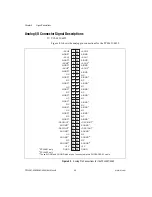
Страница 36: ...D NC AIGND NC AIGND NC AIGND NC AIGND ACH3 2 AIGND ACH2 2 AIGND ACH1 AIGND ACH0 DGND AOGND1 NC NC AOGND 1 DAC1OUT 1 AOGND 1 5 V AOGND 1 DAC0OUT 1 AIGND NC AIGND NC AIGND NC AIGND NC AIGND NC AIGND NC...

Страница 37: ...ilable only on the PCI 4451 DAC0OUT DAC0OUT Output Analog Output Channel 0 This pin supplies the analog inverting output channel 0 This pin is available only on the PCI 4451 DAC1OUT DAC1OUT Output Ana...

Страница 38: ...4 V 100 pA AIGND AI DAC0OUT AO 22 to DAC0OUT 4 55 k to AOGND Short circuit to DAC0OUT ground 16 7 mA at 10 V DAC0OUT AO 22 to DAC0OUT 4 55 k to AOGND Short circuit to DAC0OUT ground 16 7 mA at 10 V DA...

Страница 39: ...CGND NC CGND NC CGND NC CGND AI_SHLD3 2 CGND AI_SHLD2 2 CGND AI_SHLD1 CGND AI_SHLD0 DGND CGND NC NC CGND DAC1OUT 1 CGND 5 V CGND DAC0OUT 1 CGND NC CGND NC CGND NC CGND NC CGND NC CGND NC CGND NC CGND...

Страница 40: ...a separate purpose DAC0OUT AOGND Output Analog Output Channel 0 This pin supplies the analog non inverting output channel 0 This pin is available only on the PCI 4453 Analog Output Ground AOGND is th...

Страница 41: ...Sink mAat V Rise Time ns Bias ACH 0 3 AI 1 M inparallelwith 50 pF to AIGND 42 4 V 42 4 V 100 pA AO_SHLD 0 3 CGND DAC0OUT AO 22 to AOGND Short circuit to ground 16 7 mA at 10 V DAC1OUT AO 22 to AOGND S...
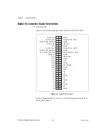
Страница 42: ...f the 68 pin connector NC NC NC NC NC NC NC 5 V 5 V 5 V DIO3 DIO4 DIO2 DIO0 DIO6 DIO7 CONVERT PFI1 TRIG2 PRETRIG PFI3 GPCTR1_SOURCE GPCTR1_OUT PFI7 PFI6 WFTRIG PFI8 GPCTR0_SOURCE GPCTR0_OUT FREQ_OUT D...

Страница 43: ...D Input Output TRIG1 As an input this is a source for the data acquisition trigger As an output this signal can drive external applications to indicate that a trigger on the device has occurred TRIG1...

Страница 44: ...nsition indicates the initiation of the waveform generation In LabVIEW referred to as AO Start Trigger for both input and output PFI7 DGND Input PFI7 This is one of the PFIs PFI8 GPCTR0_SOURCE DGND In...

Страница 45: ...pu CONVERT DO 3 5 at Vcc 0 4 5 at 0 4 1 5 50 k pu PFI3 GPCTR1_SOURCE DIO Vcc 0 5 3 5 at Vcc 0 4 5 at 0 4 1 5 50 k pu PFI4 GPCTR1_GATE DIO Vcc 0 5 3 5 at Vcc 0 4 5 at 0 4 1 5 50 k pu GPCTR1_OUT DO 3 5...

Страница 46: ...but connecting AIGND to other earth connected grounds is not recommended AIGND is not directly available if you are using a BNC 2140 accessory Figure 4 4 shows a diagram of the analog input stage of...

Страница 47: ...l has a high output impedance greater than 1 k and is floating you can use an SE configuration and tether the signal minus to AIGND to reduce common mode interference You can make the DIFF and SE conn...

Страница 48: ...plug the computer into the same power system Nonisolated outputs of instruments and devices that plug into the building power system fall into this category The difference in ground potential between...

Страница 49: ...the pair to AOGND is not the same the connection is unbalanced but the difference between the plus and minus terminals is still equal to the desired signal If the minus side is grounded the plus volta...

Страница 50: ...re 4 7 Figure 4 7 Analog Output Channel Block Diagram for the PCI 4453 The analog output stage is single ended only This means that the devices or loads receiving signals should not have their signal...

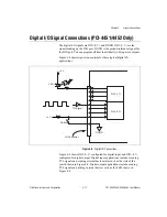
Страница 51: ...or outputs Figure 4 8 shows signal connections for three typical digital I O applications Figure 4 8 Digital I O Connections Figure 4 8 shows DIO 0 3 configured for digital input and DIO 4 7 configure...

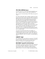
Страница 52: ...PFI0 through PFI9 excluding PFI2 and PFI5 and through the RTSI bus See Figure 3 9 RTSI Bus Signal Connection for a list of these signals These signals are explained in detail in the next section Prog...

Страница 53: ...lling The detection requirements for each timing signal are listed within the section that discusses that individual signal In edge detection mode the minimum pulse width required is 10 ns This applie...

Страница 54: ...lection for either rising or falling edge The selected edge of the PFI0 TRIG1 signal starts the data acquisition sequence for both posttriggered and pretriggered acquisitions The PCI 4451 4452 support...

Страница 55: ...TRIG2 is received the device acquires a fixed number of scans and the acquisition stops After PFI1 TRIG2 is received any additional PFI1 TRIG2 signals are ignored until the acquisition is restarted T...

Страница 56: ...the WFTRIG signal starts the waveform generation for the DACs As an output the WFTRIG signal reflects the trigger that initiates waveform generation This is true even if the waveform generation is ex...

Страница 57: ...ming requirements for the GPCTR0_SOURCE signal Figure 4 12 GPCTR0_SOURCE Signal Timing The maximum allowed frequency is 20 MHz with a minimum pulse width of 23 ns high or low There is no minimum frequ...

Страница 58: ...ows the timing of the GPCTR0_OUT signal Figure 4 13 GPCTR0_OUT Signal Timing GPCTR0_UP_DOWN Signal PCI 4451 4452 Only You can input this signal on the DIO6 pin It is not available as an output on the...

Страница 59: ...elect some external source GPCTR1_GATE Signal PCI 4451 4452 Only Any PFI pin can receive as an input the GPCTR1_GATE signal which is available as an output on the PFI4 GPCTR1_GATE pin As an input the...

Страница 60: ...requirements for the GPCTR1_OUT signal Figure 4 15 GPCTR1_OUT Signal Timing GPCTR1_UP_DOWN Signal PCI 4451 4452 Only This signal can be received as an input on the DIO7 pin and is not available as an...

Страница 61: ...SOURCE signal The GATE signal must be valid either high or low for at least 10 ns before the rising or falling edge of a SOURCE signal for the GATE to take effect at that SOURCE edge as shown by tgsu...

Страница 62: ...ccuracy of measurements made with your PCI 445X if you do not take proper care when running signal wires between signal sources and the device For more information refer to National Instruments Applic...

Страница 63: ...his type of wire the signals attached to the ACHx and ACHx inputs are twisted together and then covered with a shield You then connect this shield only at one point to the signal source ground This ki...

Страница 64: ...offset and gain errors The four levels of calibration available are described in this chapter The first level is the fastest easiest and least accurate whereas the last level is the slowest most diffi...

Страница 65: ...rily in relative measurements you can ignore a small amount of gain error and self calibration should be sufficient If you calibrate your PCI 4451 4452 while it is connected to a BNC 2140 accessory se...

Страница 66: ...e this type of recalibration every year If you require factory recalibration send your PCI 445X back to National Instruments National Instruments will send the device back to you with a new calibratio...

Страница 67: ...CI 4451 has two identical analog input channels The PCI 4452 has four identical analog input channels An analog input channel is illustrated in Figure 4 4 Analog Input Stage of the PCI 4451 4452 These...

Страница 68: ...he range of the ADCs Then digital antialiasing filters automatically adjust their cutoff frequency to remove frequency components above half the programmed sampling rate These filters cause a delay of...

Страница 69: ...usually made during offset calibration which is described in Chapter 5 Calibration Calibration The PCI 445X analog inputs have calibration adjustments Onboard calibration DACs remove the offset and ga...

Страница 70: ...ls go into the sampler a lowpass filter is applied to signals before they reach the sampler The PCI 445X includes two stages of anti alias filtering in each input channel lowpass filter This filter ha...

Страница 71: ...frequency or within one Nyquist bandwidth of multiples of 128 times the sample rate The analog filter in each channel rejects possible aliases mostly noise from signals that lie near these multiples F...

Страница 72: ...aliased into the passband region of the digital filter and is not attenuated The purpose of the analog filter is to remove these higher frequency components near multiples of the oversampling rate be...

Страница 73: ...or the PCI 4453 4454 in Figure 6 4 For frequencies not near multiples of the oversample rate the rejection is better than 85 dB Figure 6 3 Alias Rejection at the Oversample Rate for the PCI 4451 4452...

Страница 74: ...ta to have high frequency energy This energy is spread throughout the frequency spectrum and because the clipping happens after the antialiasing filters the energy is aliased back into the baseband Th...

Страница 75: ...n as delta sigma modulation If the data rate is 51 2 kS s each ADC actually samples its input signal at 6 5536 MS s 128 times the data rate and produces 1 bit samples that are applied to the digital f...

Страница 76: ...f the PCI 445X has a noise level of about 0 65 LSB rms this amount fluctuates The ratio of 23 170 475 0 65 is about 35647 or 91 0 dB the dynamic range but several factors can degrade the noise perform...

Страница 77: ...nput and output sample clocks are synchronized and derived from the same DDS clock The input and output clocks can differ from each other by a factor of 2 1 2 4 8 128 while still maintaining their syn...

Страница 78: ...ing in two stages First the data is digitally resampled at eight times the original sample rate then a linear phase digital filter removes almost all energy above one half the original sample rate and...

Страница 79: ...l Images a Spectrum of Sampled Signal b Spectrum of Signal After Digital Filter Frequency Amplitude F s 8 Fs 16 Fs Baseband Signal Images After the Digital Filter Frequency Amplitude Amplitude c Spect...

Страница 80: ...of the DAC however has a large amount of quantization noise at higher frequencies and as described in the Anti Image Filtering section some images still remain near multiples of eight times the sample...

Страница 81: ...floor drops from about 92 dB below full scale to about 120 dB below full scale Upon receiving any nonzero data the DAC instantly reverts to normal mode Mute mode is designed to quiet the background n...

Страница 82: ...curacy Note Be sure to keep the cover on your computer to maintain forced air cooling Analog Input Channel Characteristics Number of channels Resolution 16 bits Type of ADC Delta sigma 128 times overs...

Страница 83: ...samples Data transfers DMA programmed I O interrupt Transfer Characteristics INL relative accuracy 2 LSB DNL 0 5 LSB typ 1 LSB max no missing codes Device Gain Full scale Range Peak Linear Log 4451 44...

Страница 84: ...50 pF to AIGND Flatness relative to 1 kHz 3 dB bandwidth 0 493 fs Input coupling AC or DC software selectable AC 3 dB cutoff frequency 3 4 Hz Device Gain Max Offset 4451 4452 20 dB 30 mV 10 dB 10 mV...

Страница 85: ...or certified to operate beyond 42 4 V Inputs protected ACH0 ACH1 ACH2 ACH3 Common mode rejection ratio CMRR Device Gain Common Mode Range 4451 4452 Gain 0 dB both and should remain within 12 V of AIG...

Страница 86: ...only at Gain 50 dB or 60 dB PCI 4453 4454 Idle channel noise 90 dBFS Dynamic Characteristics Alias free bandwidth DC to 0 464 fs Alias rejection 80 dB 0 536 fs fin 63 464 fs Spurious free dynamic rang...

Страница 87: ...ins same configuration for all input channels Signal delay 42 sample periods any sample rate time from when signal enters analog input to when digital data is available Onboard Calibration Reference D...

Страница 88: ...16 bits Type of DAC Delta sigma 64 times oversampling Sample rates 1 25 to 51 2 kS s in increments of 47 684 S s Frequency accuracy 25 ppm Output signal range software selectable for PCI 4451 FIFO buf...

Страница 89: ...d may be shorted together indefinitely PCI 4453 yes output may be shorted to AO_SHLD or ground indefinitely Outputs protected PCI 4451 DAC0OUT DAC1OUT PCI 4453 DAC0OUT DAC1OUT Idle channel noise 91 dB...

Страница 90: ...to when analog signal appears at output terminals Digital I O PCI 4451 4452 Only Number of channels 8 input output Compatibility TTL CMOS Digital logic levels Power on state Input high impedance Data...

Страница 91: ...Min source pulse duration 10 ns edge detect mode Min gate pulse duration 10 ns edge detect mode Data transfers DMA interrupts programmed I O DMA modes Scatter gather Triggers Analog Trigger Source PC...

Страница 92: ...ctor 4 65 to 5 25 VDC at 1 0 A Digital I O connector 4 65 to 5 25 VDC at 1 0 A PCI 4452 Requirements 5 V 2 2 A idle 2 5 A active 12 V 150 mA typical not including momentary relay switching 12 V unused...

Страница 93: ...65 to 5 25 VDC at 1 0 A Physical Dimensions not including connectors 10 65 by 31 19 by 1 84 cm 4 19 by 12 28 by 0 73 in Analog I O connector 68 pin VHDCI female type PCI 4451 4452 Digital I O connect...

Страница 94: ...l SHC68 DB25 cable It also illustrates the pin connections for the optional 68 pin digital accessories for the PCI 4451 and PCI 4452 devices Figure B 1 DB 25 Pinout for the SHC68 DB25 Cable 5 V GND DA...

Страница 95: ...GPCTR1_SOURCE GPCTR1_OUT PFI4 GPCTR1_GATE PFI7 PFI6 WFTRIG UPDATE PFI8 GPCTR0_SOURCE GPCTR0_OUT PFI9 GPCTR0_GATE FREQ_OUT DGND DGND DGND DGND DGND DGND DGND DGND DGND DGND 5 V DGND DGND DGND DGND DGND...

Страница 96: ...estions FAQs and their corresponding answers or solutions including special sections devoted to our newest products The database is updated daily in response to new customer experiences and feedback T...

Страница 97: ...de information on local services You can access these Web sites from www ni com worldwide If you have trouble connecting to our Web site please contact your local National Instruments office or the so...

Страница 98: ...alue p pico 10 12 n nano 10 9 micro 10 6 m milli 10 3 k kilo 103 M mega 106 G giga 109 Numbers Symbols degree ohm percent positive of or plus negative of or minus per A A amperes AC alternating curren...

Страница 99: ...racy in the resulting digitized signal and reduces noise amplitude flatness a measure of how close to constant the gain of a circuit remains over a range of frequencies AO Start Trigger LabVIEW name f...

Страница 100: ...s when an input signal exceeds the input range of the amplifier clock hardware component that controls timing for reading from or writing to groups CMOS complementary metal oxide semiconductor CMRR co...

Страница 101: ...nt a digital or analog output channel is capable of sourcing or sinking while still operating within voltage range specifications current sinking the ability of a DAQ device to dissipate current for a...

Страница 102: ...igma modulating ADC a high accuracy circuit that samples at a higher rate and lower resolution than is needed and by means of feedback loops pushes the quantization noise above the frequency range of...

Страница 103: ...al drivers software that controls a specific hardware device such as a DAQ device or a GPIB interface device DSA dynamic signal acquisition dynamic range the ratio of the largest signal level a circui...

Страница 104: ...the effect of latencies associated with getting the data from system memory to the DAQ device filtering a type of signal conditioning that allows you to attenuate unwanted portions of the signal you a...

Страница 105: ...sition and gather data at a known position in time relative to a trigger signal high impedance in logic circuits designed to have three possible states 0 1 and hi Z the hi Z high impedance state effec...

Страница 106: ...with respect to ground is proportional to the difference between the voltages at its two inputs interrupt a computer signal indicating that the CPU should suspend its current task to service a design...

Страница 107: ...se to the equation R KS where R response S stimulus and K a constant linearization a type of signal conditioning in which software linearizes the voltage levels from transducers so the voltages can be...

Страница 108: ...nents higher than half the frequency at which it is sampled then the original signal can be recovered without distortion O offset binary format a method of digitally encoding sound that represents the...

Страница 109: ...nnection on a computer or a remote controller 2 a digital port consisting of four or eight lines of digital input and or output posttriggering the technique used on a DAQ device to acquire a programme...

Страница 110: ...ude RSE See SE RTSI bus real time system integration bus the National Instruments timing bus that connects DAQ devices directly by means of connectors on top of the boards for precise synchronization...

Страница 111: ...equire dip switches or jumpers to configure resources on the devices also called Plug and Play devices synchronous 1 hardware a property of an event that is synchronized to a reference clock 2 softwar...

Страница 112: ...ystem for digitally encoding sound that stores the amplitude values as a signed number with silence represented by a sample with a value of 0 For example with 8 bit sound samples two s complement valu...

Страница 113: ...hardware and or software elements typically used with a PC that has the functionality of a classic stand alone instrument 2 a LabVIEW software module VI which consists of a front panel user interface...

Страница 114: ...21 EXTSTROBE signal 4 21 to 4 22 PFI0 TRIG1 EXT_TRIG signal 4 20 PFI1 TRIG2 PRETRIG signal 4 21 typical posttriggered acquisition figure 4 19 typical pretriggered acquisition figure 4 20 ADC 6 9 to 6...

Страница 115: ...e filtering 6 12 to 6 13 calibration 6 14 DAC 6 14 mute feature 6 15 analog power connections 4 16 analog trigger 3 8 to 3 12 above high level analog triggering mode figure 3 9 below low level analog...

Страница 116: ...onnectors See I O connectors conventions used in manual xi xii CONVERT signal digital I O pin assignments table 4 9 digital I O signal summary table 4 11 timing connections 4 21 custom cables analog a...

Страница 117: ...criptions pin assignments table 4 9 to 4 10 pin connections figure 4 8 signal summary table 4 11 digital power connections 4 18 digital trigger specifications A 10 DIO 0 7 signal digital I O pin assig...

Страница 118: ...ut 3 4 to 3 6 input mode 3 4 input polarity and range 3 4 to 3 6 input range selection considerations 3 5 to 3 6 analog output 3 6 to 3 8 analog trigger 3 8 to 3 12 block diagrams analog function 3 2...

Страница 119: ...1 5 unpacking 1 3 PFI0 TRIG1 EXT_TRIG signal digital I O pin assignments table 4 9 digital I O signal summary table 4 11 timing connections 4 20 PFI1 TRIG2 PRETRIG signal digital I O pin assignments...

Страница 120: ...al summary table 4 11 RTSI bus signal connection figure 3 12 RTSI clocks 3 14 RTSI trigger lines overview 3 12 signal connection figure 3 12 S sample rate and device configuration 3 15 sample update c...

Страница 121: ...A 12 power requirements A 11 to A 12 timing I O A 9 to A 10 T technical support resources C 1 to C 2 theory of operation See analog operation theory timing connections 4 18 to 4 28 acquisition timing...

Страница 122: ...0 U unpacking PCI 445X 1 3 update clock frequency selecting 3 14 to 3 15 update rate and device configuration 3 15 UPDATE signal digital I O pin assignments table 4 10 digital I O signal summary table...

Отзывы: