


SECTION 3
ELECTRICAL CONTENTS
ELECTRICALTROUBLESHOOTING GUIDE
1. Power check flow
2. Preamp operation flow
DETAILS AND WAVEFORMS ON SYSTEM TEST AND DEBUGGING
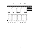
1. SYSTEM 11MHz CLOCK
2. AT89C51 reset signal
3. Volume control DATA and CLOCK
4. REC(ZONE) select DATA and CLOCK
5. Input select DATA and CLOCK
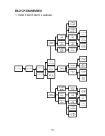
BLOCK DIAGRAMS
1. POWER DISTRIBUTE DIAGRAM
2. PREAMP SIGNAL PATH
3. SYSTEM CONTROL PATH
CIRCUIT DIAGRAMS
1. POWER AMPLIFIER BOARD Circuit DIAGRAM
2. PREAMP BOARD Circuit DIAGRAM
3. STANDBY AND SPEAKER BOARD Circuit DIAGRAM
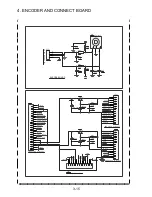
4. ENCODER AND CONNECT BOARD Circuit DIAGRAM
5. FRONT PANEL BOARD Circuit DIAGRAM
6. BALANCE INPUT BOARD Circuit DIAGRAM
7. POWER BOARD Circuit DIAGRAM
PRINTED CIRCUIT DIAGRAMS
1. Preamp Main board(PREM)
2. Preamp LCH input board(PREL)
3. Preamp tone control board(PRET)
4. Power supply board(PSU)
5. Balance amplifier board(BAL)
6. Connect board(CON)
7. Encoder board(ENC)
8. Speaker board(SPK)
9. Front pannel board(FPP)
10. Standby board Bottom(STBB)
11. Standby board top(STBT)
12. Left Channel PCB
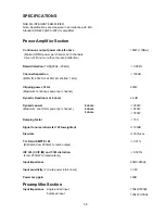
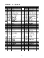
3-2
3-2,3
3-4,5
3-6
3-6
3-6
3-7
3-7
3-8
3-9
3-9
3-10
3-11
3-12
3-12
3-13
3-14
3-15
3-16
3-17
3-18
3-19
3-19
3-20
3-20
3-21
3-22
3-23
3-23
3-23
3-24
3-25
3-26
3-27
3-28
3-29
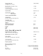
3-1
13. Right Channel PCB
14. Preamp Module
PCB
Содержание Masters M3
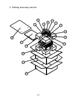
Страница 12: ...P006 P005 P001 P002 P003 P004 P008 P007 P011 P009 P013 P016 P015 P014 P012 P010 2 Packing accessory section 2 3...
Страница 20: ...DETAILS AND WAVEFORMS ON SYSTEM TEST AND DEBUGGING 1 SYSTEM 11MHz CLOCK 2 AT89C51 reset is high active 3 6...
Страница 21: ...3 volume control DATA and CLOCK 4 REC ZONE select DATA and CLOCK 3 7...
Страница 22: ...5 Input select DATA and CLOCK 3 8...