


6.2
Module Pin Out
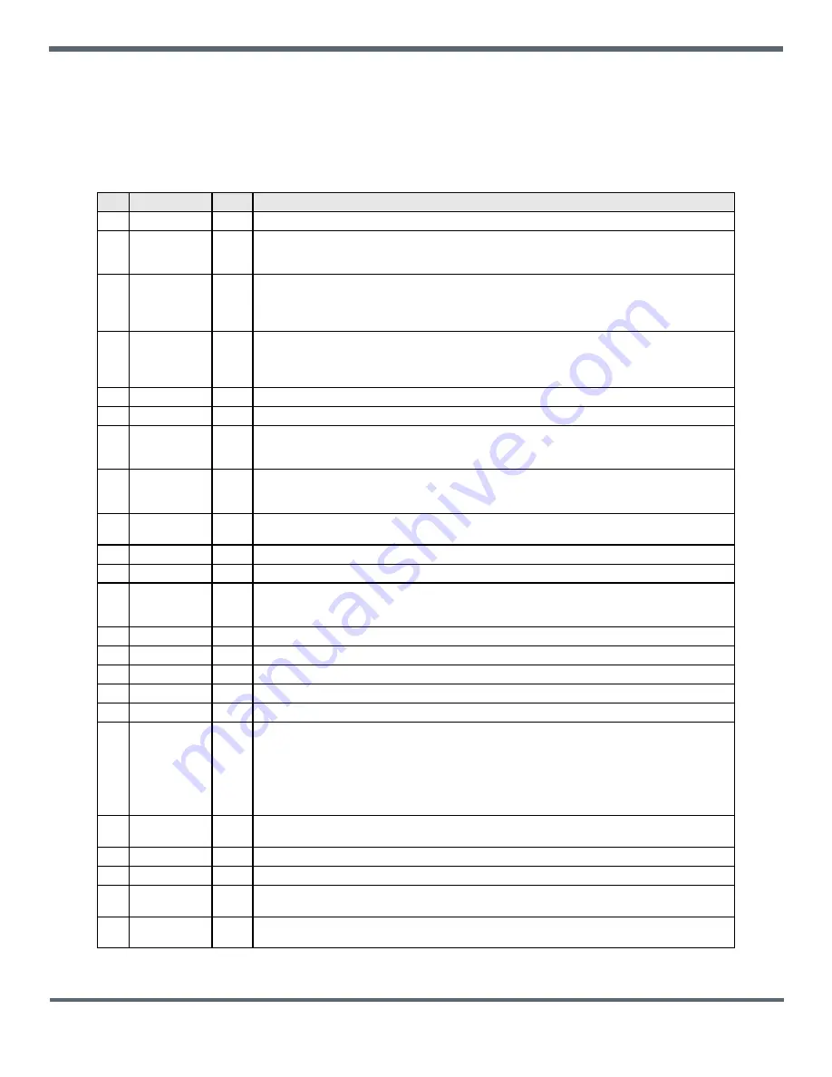
Electrical connections to the DNT90MC are made through the I/O pads and through the I/O pins on the DNT90MP. The
hardware I/O functions are detailed in the table below:
Pin
Name
I/O
Description
1
GND
-
Power supply and signal ground. Connect to the host circuit board ground.
2
ACT
(DIAG_TX)
O
(O)
This pin’s default configuration is transmitter activity (ACT) output. The ACT signal is asserted
whenever any data packet other than just an ACK is transmitted. The alternate function for this pin
is the diagnostic serial port output.
3
/DCD
(DIAG_RX)
O
(I)
The /DCD signal is asserted when a DNT90M receives a valid packet. If a radio is transmitting data
and receiving ACKs, both the ACT and /DCD signals will be asserted. If a radio is receiving pack-
ets only, the /DCD signal will be asserted. The alternate function for this pin is the diagnostic serial
port input.
4
GPIO0
I/O
Configurable digital I/O port 0. When configured as an input, an internal pull-up resistor can be
selected and direct interrupt from sleep can be invoked. When configured as an output, the power-
on state is configurable. In sleep mode the pin direction, input pull-up selection or output state are
also separately configurable.
5
RADIO_TXD
O
Serial data output from the radio.
6
RADIO_RXD
I
Serial data input to the radio.
7
GPOI4
(/HOST_CTS)
I/O
(O)
GPIO4 with the same configuration options as GPIO2. Alternate pin function is UART/SPI flow
control output. The module sets this line low when it is ready to accept data from the host on the
RADIO_RXD or MOSI input. When the line goes high, the host must stop sending data.
8
GPIO5
(/HOST_RTS)
I/O
(I)
GPIO5 with the same configuration options as GPIO2. Alternate pin function is UART/SPI flow
control input. The host sets this line low to allow data to flow from the module on the RADIO_TXD
pin. When the host sets this line high, the module will stop sending data to the host.
9
DAC0
O
12-bit DAC 0 output. Full scale can be referenced to the voltage at pin 25, or the 3.3 V regulated
module bus voltage.
10
GPIO2
I/O
Configurable digital I/O port 2. Same configuration options as GPIO0.
11
GPIO1
I/O
Configurable digital I/O port 1. Same configuration options as GPIO0.
12
GPIO3
(DAV)
I/O
(O)
Default pin function is GPIO3 with the same configuration options as GPIO0. When SPI slave
mode operation is enabled, a logic high on this pin indicates when data is available to be clocked
out by the SPI master.
13
DAC1
O
12-bit DAC 1 output. Same specifications and configuration options as DAC0.
14
VCC
I
Power supply input, +3.3 to +5.5 Vdc.
15
GND
-
Power supply and signal ground. Connect to the host circuit board ground.
16
GND
-
Power supply and signal ground. Connect to the host circuit board ground.
17
/RESET
I
Active low module hardware reset.
18
ADC0
I
ADC input 0. This pin is a direct ADC input when the ADC is operating in single-ended mode, or
the differential negative input for positive inputs applied to ADC1 or ADC2 when the ADC is operat-
ing in differential mode. Full-scale reading can be referenced to Pin 25 for ratiometric measure-
ments. For absolute measurements, the ADC can use the regulated supply voltage divided by 1.6
(about 2.06 V), or an external voltage applied to Pin 25. In single-ended mode, ADC measure-
ments are 11-bit unsigned values with full scale nominally 2.7 V when referenced to a 2.7 V input
on Pin 27. In differential mode, ADC measurements are 12-bit signed values.
19
ADC1
I
ADC input 1. Direct input when the ADC is operating in single-ended mode, positive differential
input relative to ADC0 when the ADC is operating in differential mode.
20
MISO
I/O
This pin is the SPI master mode input or slave mode output.
21
MOSI
I/O
This pin is the SPI master mode output or slave mode input.
22
/SS
I/O
SPI active low slave select. This pin is an output when the module is operating as a master, and an
input when it is operating as a slave.
23
SCLK
I/O
SPI clock signal. This pin is an output when operating as a master, and an input when operating as
a slave.
©2012 by Murata Electronics N.A., Inc.
DNT90M Integration Guide (2012/09/17)
Page 24 of 74
www.murata.com


