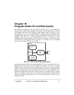
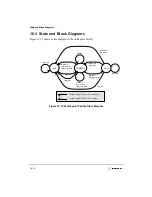
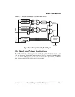

Chapter 16. Programmable I/O and Watchpoint
16-9
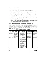
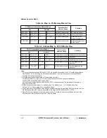
Watchpoint Registers
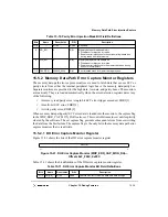
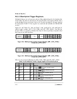
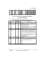
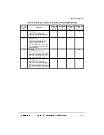
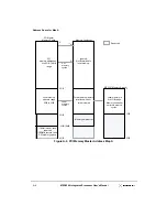
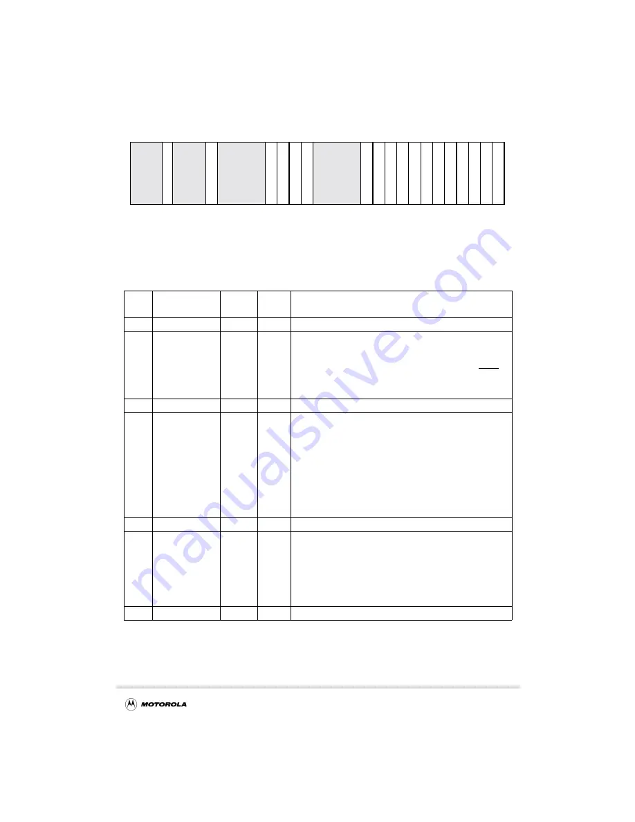
Figure 16-11. Watchpoint Control Register (WP_CONTROL)—
Offsets 0xF_F048, 0xF48
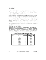
Table 16-7 shows the bit field definitions for WP_CONTROL.
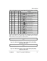
Table 16-7. Watchpoint Control Register Bit Field Definitions
Bits
Name
Reset
Value
R/W
Description
31–29
—
0b000
R
Reserved
28
DEBUG_ADDR_
x
RW
Debug address disable. See Section 15.3, “Memory Debug
Address,” for more information.
0 Debug address facility is enabled
1 Debug address facility is disabled
Note that the reset value of this bit is determined by the GNT4
signal. See Section 2.4, “Configuration Signals Sampled at
Reset,” for more information.
27–25
—
0b000
R
Reserved
24
WP_RUN
0
R/W
The watchpoint run bit is used to start and stop a watchpoint
scan. This is the only watchpoint register bit that should be
changed by software while the watchpoint facility is enabled
(WP_RUN = 1). This bit can also be toggled externally by pulsing
the TRIG_IN signal if the watchpoint facility is not in the HOLD
state.
When the watchpoint facility is in the HOLD state, pulsing
TRIG_IN causes the watchpoint facility to wake up and continue
or conclude its scan as programmed.
0 Start a watchpoint scan.
1 Stop a watchpoint scan.
23–20
—
0b0000
R
Reserved
19–16
WP2_CNT[0–3]
0b0000
R/W
The watchpoint #2 counter field sets the initial value of the
countdown counter for watchpoint #2. This counter is only used in
watchpoint waterfall mode (WP_MODE = 0b01).
0000 16
0001 1
0010 2
...
1111 15
15–12
—
0b0000
R
Reserved
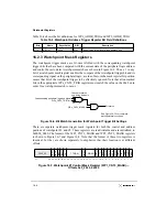
0 0 0
DEB
UG_
0 0 0
WP_R
UN
0 0 0 0
WP2_CNT0
WP2_CNT1
WP2_CNT2
WP2_CNT3
0 0 0 0
WP1_CNT0
WP1_CNT1
WP1_CNT2
WP1_CNT3
WP_TRIG0
WP_TRIG1
WP_MODE0
WP_MODE1
WP_D
A
TC0
WP_D
A
TC1
WP_CONT
WP_TRIG_HOLD
31 30 29 28 27 26 25
24
23
22
21
20
19
18
17
16
15
14
13
12
11
10
9
8
7
6
5
4
3
2
1
0
Содержание MPC8240
Страница 1: ...MPC8240UM D Rev 1 1 2001 MPC8240 Integrated Processor User s Manual ...
Страница 38: ...xviii MPC8240 Integrated Processor User s Manual TABLES Table Number Title Page Number ...
Страница 48: ...xlviii MPC8240 Integrated Processor User s Manual Acronyms and Abbreviations ...
Страница 312: ...6 94 MPC8240 Integrated Processor User s Manual ROM Flash Interface Operation ...
Страница 348: ...7 36 MPC8240 Integrated Processor User s Manual PCI Host and Agent Modes ...
Страница 372: ...8 24 MPC8240 Integrated Processor User s Manual DMA Register Descriptions ...
Страница 394: ...9 22 MPC8240 Integrated Processor User s Manual I2O Interface ...
Страница 412: ...10 18 MPC8240 Integrated Processor User s Manual Programming Guidelines ...
Страница 454: ...12 14 MPC8240 Integrated Processor User s Manual Internal Arbitration ...
Страница 466: ...13 12 MPC8240 Integrated Processor User s Manual Exception Latencies ...
Страница 516: ...16 14 Watchpoint Trigger Applications ...
Страница 538: ...B 16 MPC8240 Integrated Processor User s Manual Setting the Endian Mode of Operation ...
Страница 546: ...C 8 MPC8240 Integrated Processor User s Manual ...
Страница 640: ...INDEX Index 16 MPC8240 Integrated Processor User s Manual ...


