16-6
Watchpoint Registers
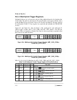
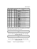
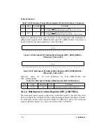
Table 16-4 shows the bit definitions for WP1_ADDR_TRIG and WP2_ADDR_TRIG.
16.2.3 Watchpoint Mask Registers
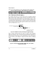
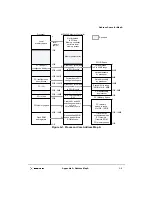
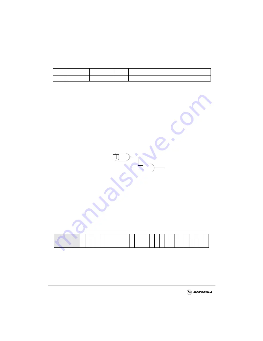
The watchpoint trigger masks are bit-wise ANDed with the corresponding watchpoint
trigger bits that have been compared with the current state of the peripheral logic address
and control buses to detect watchpoint matches as shown in Figure 16-6. Thus, a 1 in any
bit of a watchpoint mask register enables the compare of that watchpoint trigger bit and its
corresponding signal on the peripheral logic; a value of zero in the mask register bit position
causes that bit of the watchpoint trigger to be effectively ignored. Note that all unmasked
bits in the appropriate WPx_CNTL_TRIG register must match the value on the 60x bus in
order for a watchpoint match to occur.
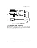
Figure 16-6. Bit Match Generation for Watchpoint Trigger Bit Settings
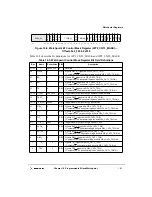
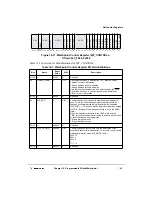
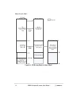
There are separate watchpoint trigger mask registers for both the control and address
portions of watchpoint #1 and #2. These registers are read/writable and are initialized to
0x0000_0000. The format of the WP1_CNTL_MASK and WP2_CNTL_MASK registers
is shown in Figure 16-7 and Figure 16-8. Note that the format of these two registers is
identical, but they are shown separately to emphasize that their location is at different
offsets.
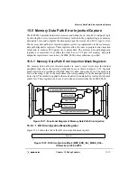
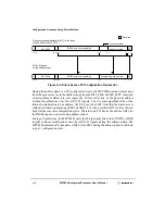
Figure 16-7. Watchpoint #1 Control Mask Register (WP1_CNTL_MASK)—
Offsets 0xF_F020, 0xF20
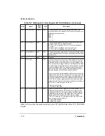
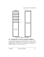
Table 16-4. Watchpoint Address Trigger Register Bit Field Definitions
Bits
Name
Reset Value
R/W
Description
31–0
A[31:0]
all 0s
R/W
Trigger value for peripheral logic address bus
WPx_CNTL_TRIG bit
Checks for match
on a bit-by-bit basis
WPx_CNTL_MASK bit
Bit match
Corresponding peripheral logic bus signal
See Figure 16-13 for complete
watchpoint match criteria.
0000_00
QREQ_
QA
CK_
BR_
BG_
TS_
TT0[0:4]
TBST_
TSIZ[0:2]
GBL_
CI_
WT_
TC0
TC1
AA
CK_
AR
TR
Y_
DBG_
TA
_
TEA_
INT_
MCP_
31
26 25
24
23
22
21
20
19
18
17
16
15
14
13
12
11
10
9
8
7
6
5
4
3
2
1
0
Содержание MPC8240
Страница 1: ...MPC8240UM D Rev 1 1 2001 MPC8240 Integrated Processor User s Manual ...
Страница 38: ...xviii MPC8240 Integrated Processor User s Manual TABLES Table Number Title Page Number ...
Страница 48: ...xlviii MPC8240 Integrated Processor User s Manual Acronyms and Abbreviations ...
Страница 312: ...6 94 MPC8240 Integrated Processor User s Manual ROM Flash Interface Operation ...
Страница 348: ...7 36 MPC8240 Integrated Processor User s Manual PCI Host and Agent Modes ...
Страница 372: ...8 24 MPC8240 Integrated Processor User s Manual DMA Register Descriptions ...
Страница 394: ...9 22 MPC8240 Integrated Processor User s Manual I2O Interface ...
Страница 412: ...10 18 MPC8240 Integrated Processor User s Manual Programming Guidelines ...
Страница 454: ...12 14 MPC8240 Integrated Processor User s Manual Internal Arbitration ...
Страница 466: ...13 12 MPC8240 Integrated Processor User s Manual Exception Latencies ...
Страница 516: ...16 14 Watchpoint Trigger Applications ...
Страница 538: ...B 16 MPC8240 Integrated Processor User s Manual Setting the Endian Mode of Operation ...
Страница 546: ...C 8 MPC8240 Integrated Processor User s Manual ...
Страница 640: ...INDEX Index 16 MPC8240 Integrated Processor User s Manual ...

